In this article, the VLSI design flow will be demonstrated. The first step in the VLSI process is the design specification, which usually comes from the client, who writes down the functionality they want to develop in the chip and the required specifications. Next, the entire design process will go through different design cycles, usually taking 6 to 24 months to complete the design, depending on the complexity within the chip. Making chips fromideasto getPhysical chip, mainly divided into three parts:Front-end design, back-end design, manufacturing。
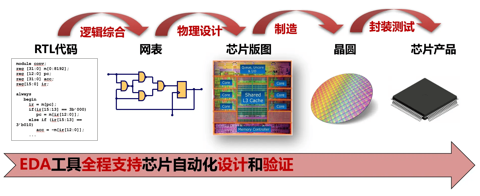
Figure 1 Chip design and production process
In integrated circuit design, the process of writing verification from Verilog/VHDL code (RTL level) and then converting it into a gate-level netlist (gate netlist) through synthesis is calledDigital front-end design. The next work is the physical implementation of the gate-level netlist, that is, converting the gate-level netlist into a layout. This process is usually calledBackend design(backend design). The process of layout manufacturing and packaging to form chip products through foundries becomesmanufacturing。
1 Overview of VLSI design process
(1) Front-end design
The front-end design process starts fromSpecifications received by the clientStart. First, RTL design engineers typically use HDL [Hardware Description Language: Hardware Description Language], such as Verilog or VHDL, converts the specification intoRTL code. These RTL codes describe the logic functions and data flow of the chip.
Once the RTL code is written, the RTL designer uses an RTL simulator to functionally verify the code. In the simulator, designers can simulate various input situations and check that the design is functioning properly. If no errors are found and the code is verified by the functional verification engineer, the RTL code can move to the next stage and this process becomesPre-simulation。
The general process is as follows:
Specification development: Develop corresponding specifications based on product requirements;
Architecture design: According to the specification requirements, design the chip architecture, divide the system functional modules, define the BUS structure, system model, manufacturing packaging and board card requirements, and output design documents;
Functional implementation and verification: According to each functional module, implement the corresponding RTL code and conduct functional simulation verification. During this period, we mainly use Debug tools and waveform simulation tools to output RTL-level Verilog code. If necessary, each IP function module needs to be integrated into SoC and functionally verified. For verification, it can be completed with the help of FPGA or hard simulation;
logical synthesis: The RTL code is logically compiled to form a state machine or truth table, and then the logic optimization design is performed to form a GTech circuit. Then the netlist is obtained through process library mapping, circuit-level simulation and formal verification are performed, and Netlist-level Verilog code is output. After synthesis, perform DFT and insert some test modules;
(2) Back-end design
Back-end design refers to the design process from the gate-level netlist to the completion of the chip layout, including logic synthesis, physical synthesis, timing analysis, timing optimization, DRC and LVS verification, design rule filling, post-simulation and other steps. Complete backend design byBackend semi-customizedwithFully customized backendIt consists of two design parts:
Fully customized back-end designIt refers to the physical unit library that is first designed according to the design requirements in the early stage of design. The physical unit library consists of a standard unit library, an IP library, and customized component units that meet special needs. This physics library provides a physical implementation basis for subsequent back-end semi-custom design.
Back-end semi-custom designIt refers to using placement and routing tools and based on the standard unit library and IP library completed in the back-end full customization stage, and completing the assembly and implementation of the entire chip based on the front-end design. This process is also calledDigital backend design(Automatic place and route-APR). Commonly used tools include IC Compiler, PrimeTime, PrimeRail, etc.
Back-end semi-custom design accounts for a major part of the design standard cell library of each unit inEqual height, no limit to width, in the unitThere are special regulations on the location of power supply, ground wire and input and output ports., making the connection between units simple and organized, and the layout regular, simplifying the design process. Of course, there are some problems with designing using standard cells: the available components are limited and it is difficult to efficiently construct complex devices (such as multipliers).
The back-end full customization process is as follows:
- Cell library design: The process library obtained from Foundary will basically contain IO, Memory and some IP, as well as PDK and unit library. However, the design of the unit library can be further optimized. First, design the unit model, conduct unit circuit layout design, extract parameters of the unit, and perform physical verification;
The back-end semi-customization process is as follows:
layout planning: Determine the shape and arrangement of circuits or modules, as well as the positions of ports and macro modules;
Power planning: Determine the location of power supply (VDD) and ground (GND);
Layout: Determine the spatial positions of all units in different modules;
clock synthesis: Determine buffering, gating, and routing of clock signals to meet specified skew and delay;
General wiring: Allocate wiring resources to connect detailed wiring and allocate wiring to specified metal layers;
Sign-off analysis: During the logic synthesis and physical design process, the circuit and layout need to be analyzed for parameter extraction, timing, power consumption, IR drop, power supply and signal integrity to ensure that the obtained circuit and layout meet the design specification constraints;
Physical verification: After obtaining the GDS layout, in addition to sign-off analysis, physical structure verification is also required, which mainly includes: design rule check (DRC), electrical rule check (ERC), layout and schematic comparison (LVS), etc. Afterwards, a final simulation is required to ensure the correctness of the entire layout function;
Among them, the steps6-10collectively referred to asphysical design. For the comprehensively obtained netlist, it is necessary to design the layout, layout, clock tree synthesis, wiring, ECO and other steps, and finally obtain the GDS layout file. Of course, in order to achieve expected PPA indicators and meet design rules, physical design often requires multiple iterations. In addition, each step of the physical design also requires formal verification to confirm functional correctness.
(3) Manufacturing
Chip manufacturing is the process of converting chip layout into chip entity, including mask making, wafer manufacturing, chip packaging and testing. The manufacturing process involves a variety of technologies, such as photolithography, ion implantation, etching, etc., as well as various measurement and testing methods, such as microscopes, scanning electron microscopes, test chips, etc.
Layout processing: After completing the physical verification, the chip design process is basically completed. Next, the layout needs to be handed over to Foundary to open the mask. It is necessary to further optimize the GDS layout and perform OPC and RET in order to enhance the resolution and reduce production deformation errors, and then use it to generate Mask;
Manufacturing packaging testing: Mainly completed by Foudary and the packaging and testing factory, and then filmed;
PCB: After completing the above steps, you can basically get a chip, which can be integrated into the required PCB for practical verification and use. The PCB-level board is also designed to address issues such as layout and wiring;
2 Detailed explanation of back-end design part
The RTL code received from the front-end engineer has nothing to do with the back-end design technology, now the next step is logical synthesis [Logic Synthesis]。
(1) Logical synthesis
In logic synthesis, a high-level description of a design (RTL code) is converted into an optimized gate-level representation given a library of standard cells and certain design constraints. The code now takes the form of a gate-level netlist of a specific standard cell library. Must be done at this stage LEC [Logic Equivalence Check : logical consistency check] to ensure that no logical changes occur during synthesis. During logic synthesis we also get various reports on timing power and design area. At this stage we will also get a SDC [Synopsys Design Constraint:Synopsys design constraints] file, which will be used in the next stage.DFT [Design For Testability : Design for testability] Inserting test logic is also done at this stage to verify the chip after manufacturing is complete.
(2) Layout and wiring
The gate-level netlist and SDC file after DFT insertion are as PnR [Place and Route : Placement and routing] and start PnR based on the standard cell library. The goal of the PnR phase is to place all standard cells, macrocells, and I/O pads with minimal area and minimal latency, and with no DRC [Design Rule Check : Design rule check] Wiring them together the wrong way. The final output of this stage is the design layout in the form of a GDSII file, which is the de facto standard for layout files in the industry.
The PnR stage is a very challenging stage with long design cycle times depending on the complexity of the chip. This phase is further divided into various sub-phases. The main stage starts from Design import [Design Import] starts, then layout planning [Floor Plan]、Power planning [Power Plan]、Layout [Placement]、CTS [Clock Tree Synthesis : Clock tree synthesis] and wiring [Routing]。
After routing, we expect the design to have met timing and all DRCs, but in modern chips it's not easy to shut down the design at this stage. So we go further into Sign off [signoff] stage.
(3) Sign off
If there are some timing violations in the backend layout design, we will conduct further ECO [Engineering Change Order : Engineering changes] stage to resolve these timing violations. In addition to timing violations, there may be things like voltage drop [IR Drop]、DRC [Design Rule Check : Design rule check] Violations and other problems, all these problems will be solved at this stage, and the final layout file without any violations will be output in GDSII format. This process is called in ASIC process Tape out [tapeout]. This is the final design stage and the GDSII files are sent to the fabrication lab for chip fabrication.
3 Areas covered by EDA tools
During the entire chip design process, the classification and content covered by the main EDA tools can be summarized into the following five major aspects:
- Design synthesis: The design process mainly includes high-level synthesis, logic synthesis, physical design, packaging design, and PCB design.
- Simulation simulation: The simulation link mainly includes: TCAD, transistor simulation, logic simulation, hardware simulation, field solver
- Verification test: The verification test link mainly includes: functional verification, formal verification, equivalence check, ATPG, BIST, physical verification
- Analytical checks: The analysis links mainly include: cross-clock domain, parasitic extraction, (static) timing analysis, power consumption analysis, temperature analysis, voltage drop analysis, signal/power integrity analysis
- Mask preparation: The masking process mainly includes: layout decomposition, OPC, RET, and mask generation.
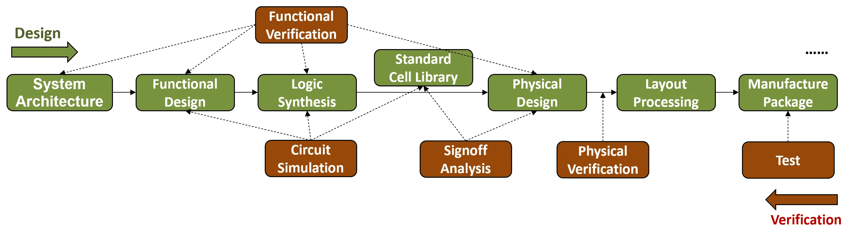
Figure 2 Main EDA tool steps
The main research and development of the iEDA research team focuses on chip logic synthesis, physical design, sign-off analysis and physical verification, as shown in the green part of the figure below:
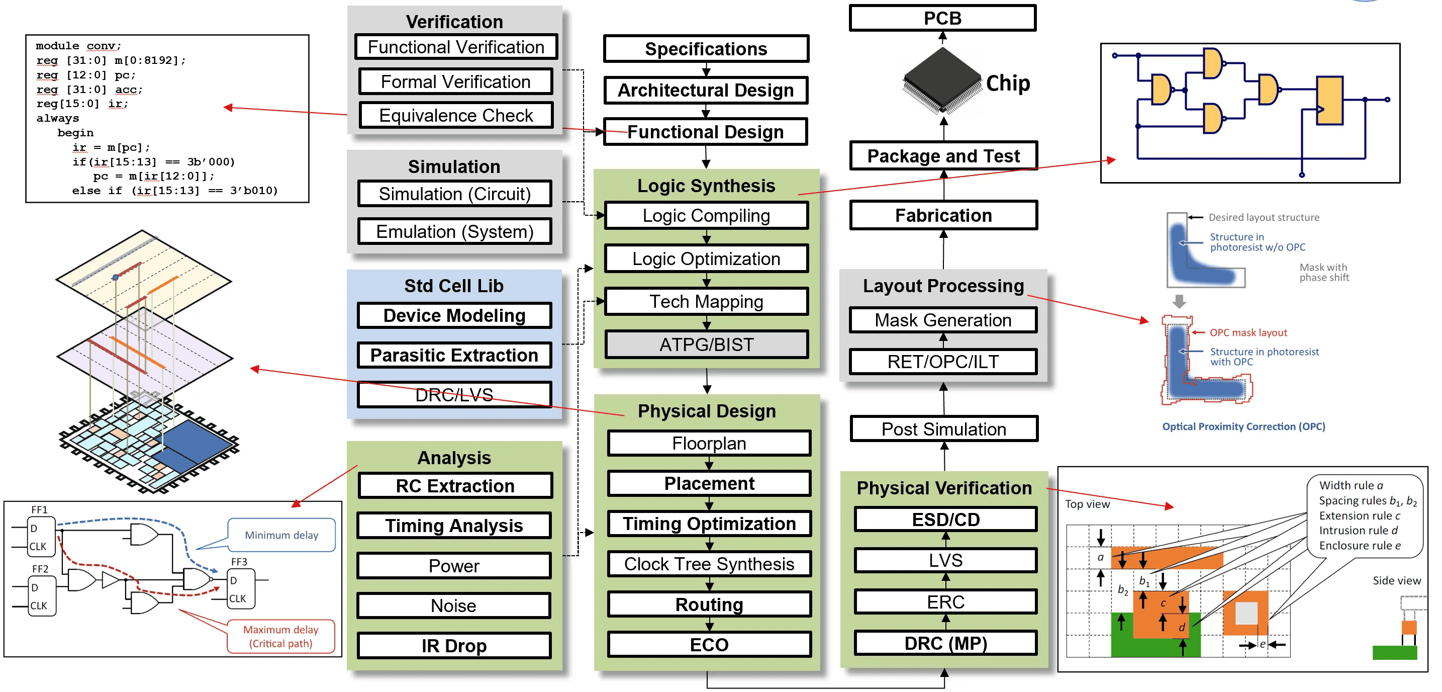
Figure 3 iEDA tool focus areas
3 The connections and differences between "wafer" "chip" "die"
1. Definition of terms:
Wafer: wafer; refers to the silicon wafer used in the production of silicon semiconductor integrated circuits because of its circular shape.
chip: chip; is a general term for semiconductor component products.
Die: Bare chip; it is a very small unit in a silicon wafer, including a fully designed single chip and some horizontal and vertical scribe groove areas adjacent to the chip.
2. Connections and differences:
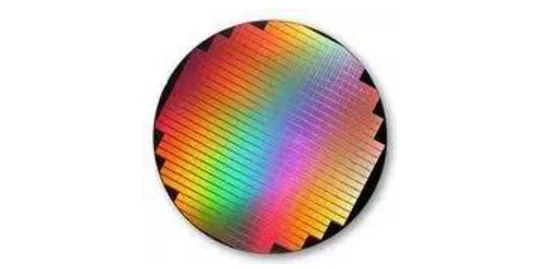
A complete wafer
A wafer is a wafer, made of pure silicon (Si). Generally divided into 6-inch, 8-inch, and 12-inch specifications, and the wafers are produced based on wafer. The scientific name of a small wafer on a wafer is die, which becomes a particle after packaging. A wafer carrying a Nand Flash wafer is first cut. After testing, the intact, stable, and sufficient-capacity die is removed and packaged to form the Nand Flash chip that is seen daily.
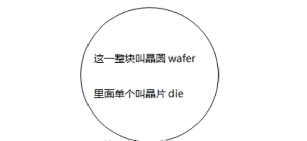
The relationship between die and wafer
After the qualified die is cut, the original wafer looks like the picture below, which is the remaining Downgrade Flash Wafer. The remaining dies are wafers of substandard quality. The black part is a qualified die, which will be packaged and made into finished NAND particles by the original factory. The unqualified part, which is the part left in the picture, will be disposed of as scrap.
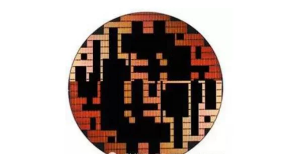
Filtered wafer
Extended information:
The life course of an integrated circuit chip: the chip company designs the chip - the chip foundry produces the chip - the packaging and testing factory performs packaging and testing - the complete machine manufacturer purchases the chip for complete machine production.
Chip supplier IDM: It is an enterprise integrating multiple industry chain links such as chip design, manufacturing, packaging and testing.
Chip supplier Fabless: It is a chip supplier without a chip processing plant. Fabless designs, develops, promotes and sells chips by itself, and outsources production-related business to professional manufacturers. Corresponding to Fabless are Foundry and packaging and testing factories, which mainly undertake the production and packaging and testing tasks of Fabless. Packaging and testing factories include ASE, Jiangsu Changdian, etc.
4 quotes
[1] https://teamvlsi.com/2020/05/asic-design-flow-overview-v1.html
[2] https://zhuanlan.zhihu.com/p/380962676
[3] https://yearn.xyz/docs/vlsi-Backend Design/70-vlsi-Backend Design-Introduction/
[4] https://zhidao.baidu.com/question/2040027.html