In one sentence, the latch-up effect means: if a certain parasitic structure appears in the chip, a certain triggering mechanism will form a low-impedance path between the power rails, resulting in a large current that damages normal circuit functions. The PNPN structure is a parasitic structure that causes the latch-up effect, but in the final analysis, the culprit is the SCR (Silicon Controlled Rectifier) structure composed of PNP and NPN. Next, starting from the SCR structure, we will describe the formation and prevention of the latch-up effect.
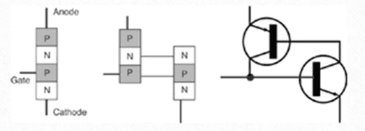
Figure 1 Left: PNPN structure; Right: SCR structure
Students who are familiar with triode principles can skip this section.The role of the transistor: to achieve small current control of large current.
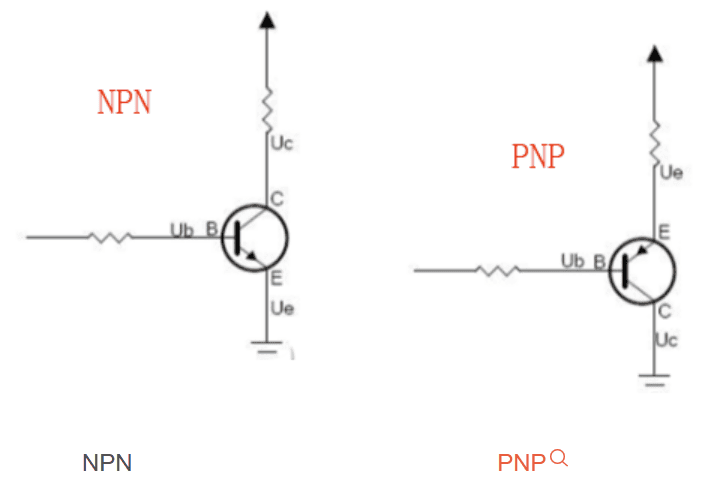
Figure 2 NPN transistor and PNP transistor
As shown in the figure below, this is an NPN transistor. N-type semiconductors have many holes, and P-type semiconductors have many free electrons. This transistor forms two PN junctions. No matter which direction the electricity is passed, the transistor will cut off. The N-type semiconductor on the left can be called the emitter region, the P-type semiconductor in the middle is called the base region, and the N-type semiconductor on the right is called the base region.
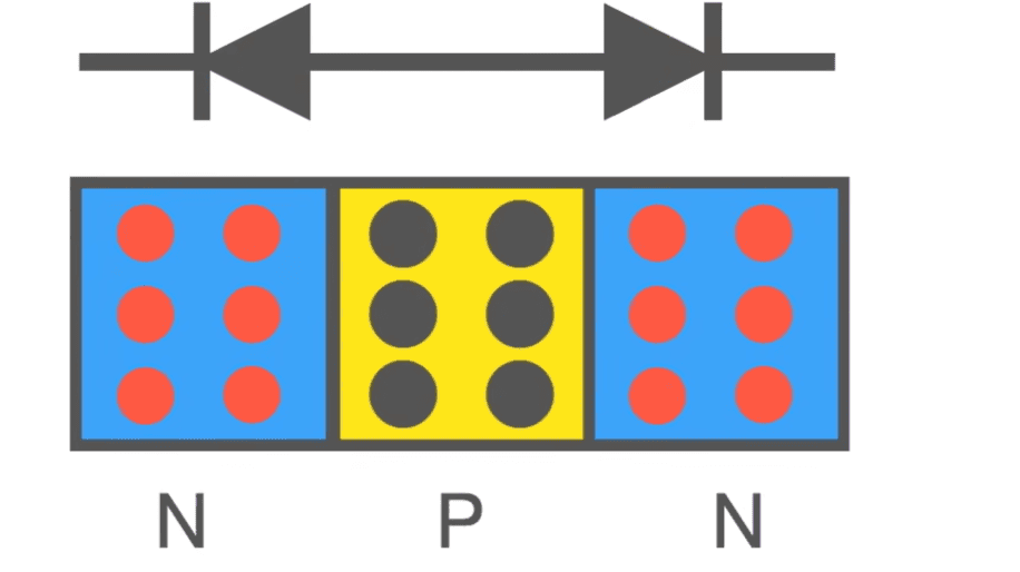
Figure 3 NPN type semiconductor
When electricity is supplied to the E-emitter region and the B-base region, a small number of electrons in the E-emitter region recombine with holes in the B-base region to form a base current. Most of the electrons will be attracted to the collector area, forming a collector current, which is the output current of the triode.
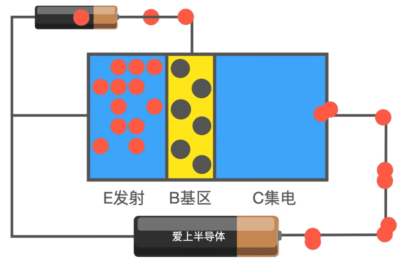
Figure 4 Transistor conduction
For more knowledge about triodes, please clickhereView the text, or clickhereCheck out the video.
2 Preliminary knowledge: Thyristor
Like a transistor or a mos tube, it is turned on when the high level is input, and turned off when the high level is withdrawn. But for thyristors, they are turned on when a high level is input, and they are still turned on when they are withdrawn. The SCR (silicon controlled rectifier) that produces the latch-up effect is a type of thyristor and is a semi-controlled device. Therefore,The thyristor can control the conduction of the circuit, but cannot control the shutdown of the circuit. Those familiar with thyristors can skip this section.
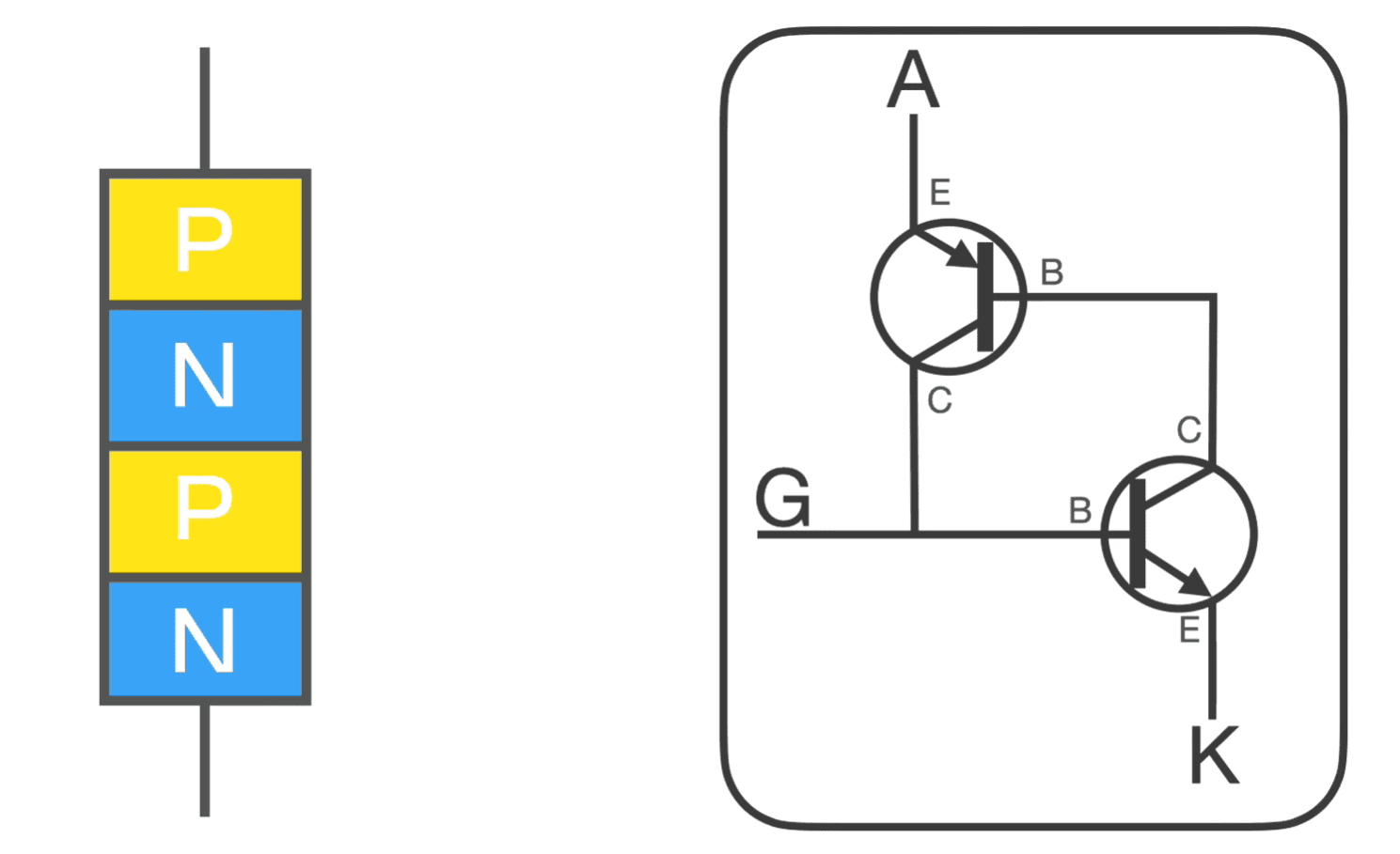
Figure 5 Structure of SCR
The PNPN structure is equivalent to connecting the triode PNP structure and the triode NPN structure together. The right side of Figure 5 is the equivalent circuit symbol of PNPN. When the voltage is connected to the G pole, Q2 is turned on, and the current of the B pole of Q1 forms a loop. Q1 is turned on, and the current output by the C pole makes the B pole form a loop, independent of the access voltage of the G pole. When the G pole voltage withdraws, the B pole loop is formed by relying on the C pole output current. Q2 is still on, so Q1 is also on, and the entire circuit is still on.
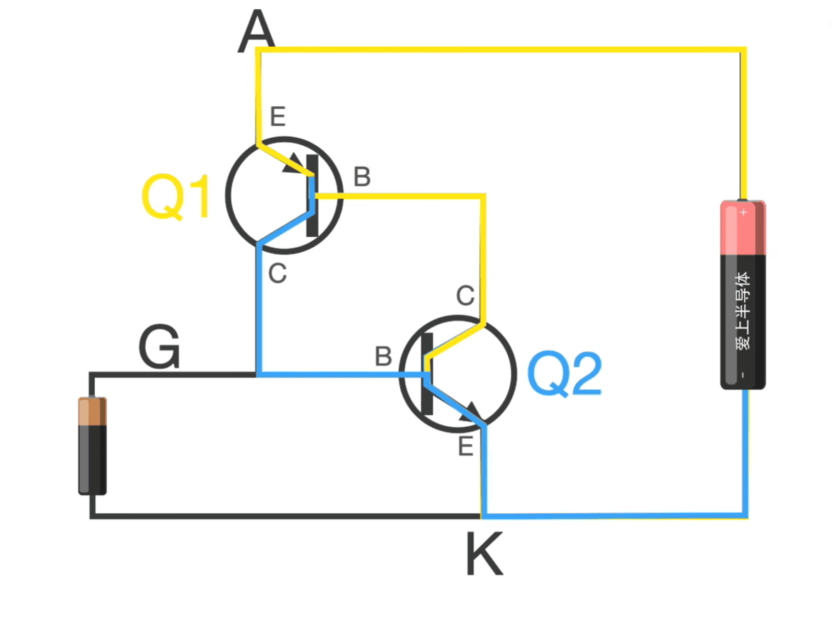
Figure 6 SCR principle
It should be noted that the A electrode is called the anode, the K electrode is called the cathode, and the G electrode is called the control electrode.
3 How latches are formed
(1) Latch generation mechanism
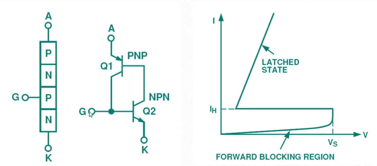
Figure 7 Latch generation mechanism
The SCR at this time is a parasitic structure and is not generated by design. It can be seen that it is composed of PNP type transistor and NPN type transistor, and is in the off state under normal circumstances. The glitch trigger on the G electrode causes the SCR to enter the Latchup, which is equivalent to forming the base current in the E and B areas of the NPN transistor. According to the characteristics of the transistor, a collector current is formed, and Q2 is turned on. Open Q1 in the same way.
Process:
The G electrode current of Q2 is injected into the Q2 base -> Q1 base emitter generates current -> Q1 turns on -> more current is injected into the Q2 base -> positive feedback is formed -> Q1Q2 is saturated. Once the Latchup is triggered, the Latchup state will not exit even if the signal on the G pole is removed.
Exit mechanism:
To exit the Latchup, either the voltage across the SCR decreases to a certain value or the current flowing is less than IH
(2) Formation of SCR structure
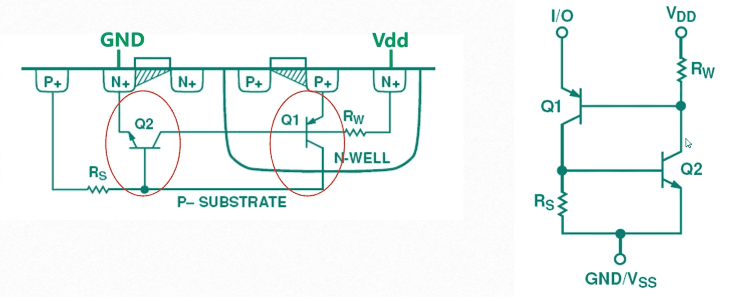
Figure 8 Formation of SCR structure
Inside a CMOS (Complementary Metal Oxide Semiconductor) circuit, two parasitic BJTs (Bipolar Transistors) are formed and connected in such a way that these BJTs form a PNPN device or SCR (Silicon Controlled Thyristor) or Thyristor.
As shown in the figure above, a pMOS device is formed on the n-type well, and an nMOS device is formed on the p-substrate area. If we look at the area below the source or drain of a pMOS device, the source or drain is formed by a P+ implant, then the n-type well, and then the p substrate below. Therefore, a parasitic PNP BJT is formed here with the emitter being the source of the pMOS, the base being the n-well and the collector being the p-substrate. Similarly, a parasitic NPN BJT is formed near the nMOS device, whose emitter is the source of the nMOS, the base is the p-substrate, and the collector is the n-type well.
These two BJTs are connected to each other in a way that makes them form a PNPN device. The base of the PNP BJT is connected to the collector of the NPN BJT and the base of the NPN BJT is connected to the collector of the NPN BJT.
A PNPN device is usually off and has very little or no current flowing through it. But once the PNPN device is triggered by its gate signal, a large current will start flowing through it, and it will continue to flow even if the gate signal is removed. The figure below shows the terminals and characteristics of the PNPN device.
Summary:
Q1 and Q2 are not designed, but formed parasitically:
- Formation of parasitic Q2 NPN: P substrate is the base, N+ well is the emitter, and other unrelated N+ wells are the collector
- Formation of parasitic Q1 PNP: N+ well is the base, P+ is the emitter, and P substrate is the collector
- After the SCR is triggered, VDD provides current. If the current is not limited, it will damage the chip.
For more latch knowledge, clickhereView the text, or clickhereCheck out the video.
2 Trigger mechanism and prevention of latch
(1) Trigger mechanism of latch
Digital chip: When the positive or negative pulse signal on the input and output pins exceeds the voltage difference of one diode of the power rail, latch-up may occur.
Analog Chips: Like amplifiers, latch-up occurs when the input exceeds the supply rails, or when the power supplies are powered up differently.
PNPN devices formed inside CMOS can be triggered in various ways. Once the PNPN device is triggered by any means, the latch-up event begins. Here are some of the main reasons.
- Noise at the output port
- Electrostatic discharge (ESD) events
- ionizing radiation
Assuming that the output voltage has exceeded VDD due to noise, then it will forward bias the transistor between the drain and n-well of the pMOS. Once this junction is forward biased, the P+ region will start injecting holes into the n-well, which will be collected by the nMOS's body contact since it is connected to GND. Therefore, this event will cause a current to flow from the drain of the pMOS to the body of the nMOS. Due to the flow of the above-mentioned current, a voltage drop will occur between the source terminal of the nMOS and the substrate below it. It will forward bias the pn junction between the source and substrate of the nMOS. This will again start injecting electrons from the N+ source into the substrate, which will be collected by the body end of the pMOS connected to VDD, as shown by the red dashed line. Therefore, eventually a chain will be initiated, and next the source side of the pMOS and the n-type well will be forward biased. In this way, both diodes are turned on and a latch-up is formed.
Similarly, if the output voltage is lower than VDD, first the junction between the nMOS's drain and the substrate will be forward biased, then it will forward bias the junction between the pMOS's source and the n-type well, and further it will forward bias the junction between the nMOS's source and the substrate, which will cause both BJTs to open and create a latch-up.
(2) Latch prevention
Before discussing prevention techniques for latch-up problems, let us first review the key factors of latch-up problems. The following two factors are crucial to the Latch-up problem.
- High resistance of n-well and p-substrate
- β1 x β2 > 1
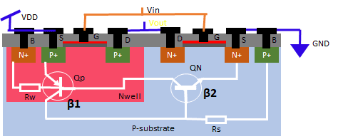
Figure 9 Formation of Latch-up
Figure 9 shows parasitic BJT formation leading to latch-up. The resistance of n-well and p-substrate can be reduced by increasing doping, but this can severely degrade device performance. However, we can reduce the gain (β) of the parasitic BJT, thereby preventing the latch-up problem. Some popular latch-up prevention techniques are as follows.
- protective ring
- well ground unit
- isolation trench
- epitaxial layer
- reverse well doping
- Combination of epitaxial layer and reverse well doping
- mFDSOI technology
- ESD protection technology
1. Protective ring:
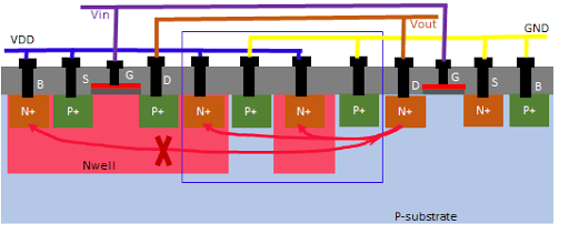
Figure 10 Protection ring
If the output voltage falls below VSS and the diode between the drain of the nMOS and the p-substrate becomes forward biased, electrons from the drain start to be injected into the substrate and are collected by the body of the pMOS. This results in a current flowing in the opposite direction to the electron flow. Ultimately the Qp transistor shown in Figure 9 is triggered. In order to break this chain, two sets of n+ implants are added to the n-well, while p+ implants are added to the p-substrate, as shown in Figure 8. These will collect electrons injected from the nMOS drain and block current flow from the nMOS drain to the pMOS body. This prevents the Qp BJT from triggering.
Similarly, if the output voltage is higher than VDD, and the drain of the pMOS starts injecting holes into the n-well and are collected by the body of the nMOS, the Qn BJT is triggered. But by adding a guard ring, these holes will be collected by the guard ring and prevent latch-up.
2. Well grounding unit:
In a groundless standard cell design, in order to prevent Latch-up, we need to ground the n-well to VDD and the p-sub to VSS. These well ground units ground the n-well to VDD and the p-sub to VSS. Figure 11 shows the cross-section of the ungrounded unit and the grounded unit, and Figure 12 shows the layout of the well grounded unit and the ungrounded standard unit.
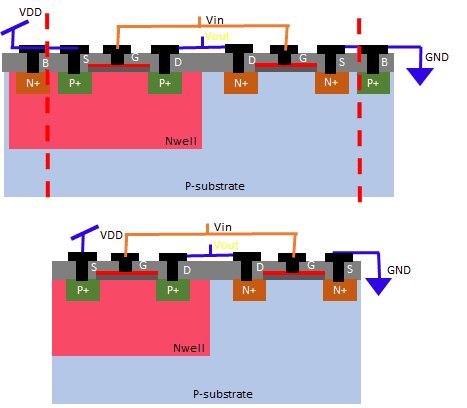
Figure 11 Cross-section of a well-grounded cell and an ungrounded cell
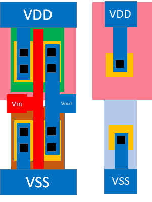
Figure 12 Layout of ungrounded cells and well-grounded cells
Well ground cells are placed at regular intervals in rows of standard cells following the maximum distance rules defined in the technology library.
3. Oxide trench isolation:
In this technology, nMOS and pMOS are isolated using buried oxide and oxide trenches. Create horizontal buried oxide deep down and then create vertical oxide trenches and connect the two together to separate the n-well and p-substrate. The oxide trench is an insulator, so the oxide trench prevents the formation of PNPN devices. Figure 13 shows a cross-section of oxide trench isolation.
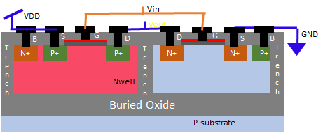
Figure 13 Cross-section of trench isolation
4. Epitaxial layer:
In this technique, a low-doped p-epitaxial layer (called P-) is grown on a P-substrate (called P+). The P-epitaxial layer provides a low-impedance path for minority carriers and prevents latch-up triggering. This technique is also called P on P+. Figure 14 shows a cross-section of CMOS using epitaxial layers.
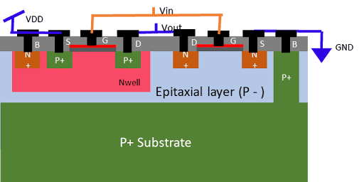
Figure 14 Cross-section of CMOS using epitaxial layers
The only problem with this technique is that growing epitaxial layers is a complicated process. As an alternative, epitaxial wafers can be used for this purpose.
5. Reverse well doping:
In a normal n-well doping process, the doping concentration is highest at the surface and decreases as the well depth increases. But in the reverse well doping process, there is very precise control of the doping concentration in depth. We have a peak doping concentration deep in the n-well, not on the surface. Figure 15 shows the doping profiles for normal doping and reverse well doping.
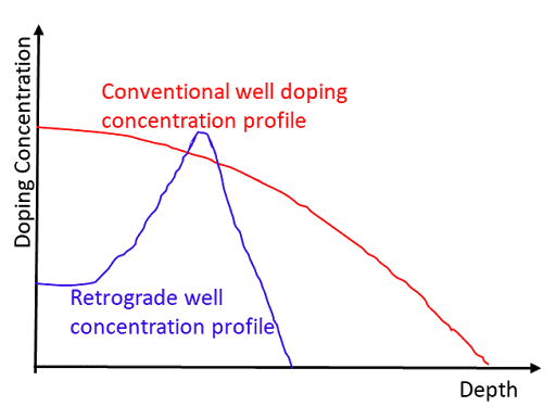
Figure 15 Doping profile of reverse gradient well doping
Reverse well doping is performed at the bottom of the normal n-well, as shown in Figure 16. This area has a high doping concentration and creates a low resistance path. The body connection taken from the N+ doping extends into this highly doped region. Therefore, a low-resistance path is formed under the n-well, preventing the PNPN device from triggering. Figure 16 shows a cross-section of reverse well doping.
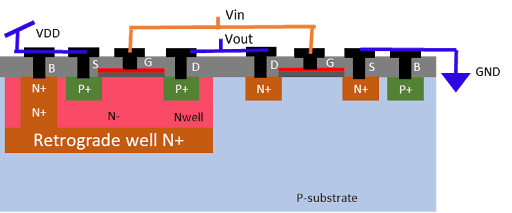
Figure 16 Reverse gradient well doped CMOS
6. Combination of epitaxial layer and reverse well doping:
We can combine the two technologies of epitaxial layer and reverse well doping, which is also a very effective method to prevent Latch-up problems, but the process is slightly complicated.
7. SOI technology:
In SOI (silicon on insulator) technology, the oxide layer lies beneath the source and drain doping and prevents the formation of parasitic BJTs. Therefore, SOI technology completely eliminates the Latch-up problem. Figure 17 shows a cross-section of CMOS in SOI technology.
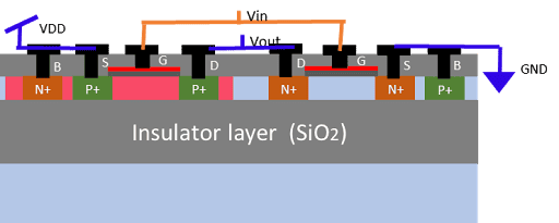
Figure 17 CMOS in SOI technology
We can combine the two technologies of epitaxial layer and reverse well doping, which is also a very effective method to prevent Latch-up problems, but the process is slightly complicated.
These are methods to prevent latch-up in CMOS technology. Each technology has its pros and cons.
Things to note are:
- Latch-up does not necessarily only occur between power rails. As long as the parasitic structure exists, door locks are likely to occur.
- Not only the CMOS process will have latch up problems, but bipolar will also have them. As long as there is a PNPN structure, it is possible to lock the door
For more knowledge about well plug units, please view Part 5, Section 3.
[1] https://teamvlsi.com/2020/05/latch-up-is-in-cmos-design.html
[2] https://teamvlsi.com/2020/05/latch-up-prevention-in-cmos-design.html