In physical design, OCV refers to the difference between the actual performance of the chip's internal circuitry and the standard expected performance. Simply put, OCV describes the changes in electrical properties between different areas within the chip. This variation may be caused by imperfections in the manufacturing process or fluctuations in environmental conditions.
In this article, we will discuss the sources of OCV [On-Chip Variation] in VLSI, why on-chip variation occurs and how to deal with on-chip variation in physical design. We will also briefly discuss AOCV [Advance On Chip Variation] and POCV [Parametric On Chip Variation].
Background:
In the ASIC design cycle, the final output sent to the fabrication lab after physical design and signoff is a .gds (Graphic Design System) file. ICs (Integrated Circuits) are fabricated on silicon wafers based on this final GDS data. A large silicon wafer is divided into various small chips, each containing an independent IC. After wafer level testing, we cut and separate each chip and package the IC.
All ICs in all chips have the same gds data, but the chip's location on the wafer is different. If all chips have the same gds, then ideally all ICs should have the same electrical characteristics. But this is not the case. The electrical characteristics of ICs manufactured in different chips will vary. Figure 1 shows a silicon wafer and the chips on the wafer.
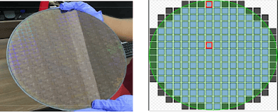
Figure 1 Silicon wafer and chips on wafer carrier
For example, let us consider the three chips shown in Figure 2 located at different locations on the wafer. Chip 1 is located in the center of the wafer, chip 3 is located at the edge of the wafer, and chip 2 is located between the center and the outer edge.
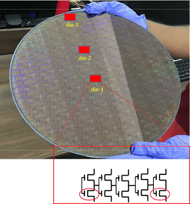
Figure 2 Wafers, chips, and transistors within a chip
So, within a wafer there are hundreds or thousands of chips, and there is variation within each chip, but also within many wafers. Or if we investigate deeper, we find that there are millions of transistors inside an IC, and all transistors within a single IC are not similar. Therefore, there is variation in transistor characteristics even within a single IC and within chips and wafers. Now an important question arises, where did all these mutations come from? What are the root causes of these variations? The answer ismanufacturing processitself is the main cause of these variations. So let's investigate the source of these variations.
Source of variation:
There are three main sources of variation, namely process, voltage and temperature. These mutations are collectively called PVT mutations. We already do PVT analysis and handle these variations when designing our ASICs, so why do we need to handle OCV separately? The answer is that not all variants can be handled in PVT analysis. Some of these are predictable and can be easily modeled as the technology matures, but some of them are very unpredictable and cannot be easily modeled. Figure 3 shows the various components of PVT and OCV variation.
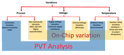
Figure 3 Variation elements under PVT and OCV
There are two types of variation in process variation, one is systematic variation and the other is non-systematic variation or random variation. Systematic variations caused by optical neighbor correction (OPC) or chemical mechanical polishing (CMP) are predictable and can be modeled in PVT variation. Non-systematic variation comes from random impurity fluctuations (RDF), line edge roughness (LER), or variation due to oxide thickness variation (OTV), which are very unpredictable and cannot be easily modeled. Or we can say that these mutations are random.
Among the voltage variations, one is caused by the variation of the external supply voltage, and the other is the variation of the internal voltage of the chip. Without an ideal voltage supply, even if the utmost care is taken in supply voltage design, there will still be a 2-5% variation in supply voltage. This type of variation is handled in PVT, but another type of variation is due to internal IR drop, which is impossible to model in PVT because it is random and design dependent. Therefore, we need to handle this voltage variation in OCV.
If we talk about temperature, then the ambient temperature in which the chip operates and the junction temperature of the transistor are key. Junction temperature is the sum of ambient temperature plus the temperature rise caused by chip power dissipation. The junction temperature is always much higher than the ambient temperature, and the characteristics of any transistor depend primarily on the junction temperature. Ambient temperature can be handled in PVT, but for junction temperature variation, we need to handle it in OCV.
Let us discuss all these variations further.
I. Process variation:
The drain current of an nMOS transistor in the linear region can be defined as

Where Id is the drain current, μn is the electron mobility, ∈ox is the dielectric constant of silicon oxide, tox is the oxide thickness, W is the width of the transistor, and L is the gate length of the transistor, as shown in Figure 4.
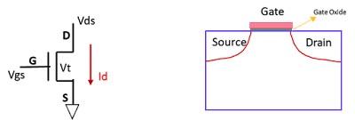
Figure 4 Pins and schematic diagram of MOS device
In the drain current equation, manufacturing process-dependent factors include:
- Gate oxide thickness (tox)
- Transistor width (W)
- Transistor length (L)
- transistor threshold voltage
Therefore, if any of the above factors changes during the manufacturing process, it will affect the drain current. The delay of a cell depends on the drain current, so the delay of a standard cell will vary due to process variations. Now look at some examples of how these parameters are affected during the manufacturing process. Figures 5 and 6 show the length and width variations associated with the photolithography process.
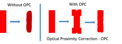
Figure 5 Photolithography nearest neighbor correction
Photolithography is a process applied to a layout prior to mask generation in order to better replicate the layout on the wafer. During this process, it is common to extend the corner edges of the layout for better yield. Figure 6 shows the general photolithography process flow.
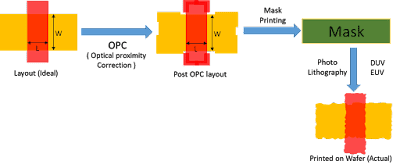
Figure 6 Photolithography process flow
Photolithography is a non-ideal process that makes it difficult to accurately print precise layouts on silicon wafers. Therefore, there is variation between the actual layout and the geometry printed on the wafer.
Here are some common types of process variations and what they mean:
Photolithography process: Photolithography is a very important process step in manufacturing chips. It uses photoresist and mask templates to define patterns and structures on the chip. Variations in the photolithography process may cause uneven or blurred exposure of the photoresist by the mask, thereby affecting the structural accuracy and dimensional accuracy on the chip.
Optical Proximity Correction (OPC): OPC is a technique used in the photolithography process to fine-tune the shape and size of the mask pattern to eliminate pattern distortion due to optical effects. However, OPC itself may also introduce variation, such as additional morphology at the edges, dimensional changes, or shape distortion.
Random Impurity Fluctuation (RDF): RDF is caused by random impurities or imperfections in the chip manufacturing process, such as doping impurities, dust particles, etc. These random impurities can cause changes in electric fields or currents inside or on the chip, causing unpredictable effects on circuit performance.
Line edge roughness (LER): LER describes the irregularity and surface roughness of the edges of metal lines when manufacturing chips. This degree of irregularity may lead to uneven current distribution and changes in circuit performance such as resistance and capacitance.
Etching: Etching is a process used to remove excess material from the surface of a chip or between layers. Variations in the etching process can lead to uneven material removal, causing changes in the shape, size, or structural profile of the structure.
Chemical mechanical polishing (CMP): CMP is used to planarize the chip surface to remove the bumps or uneven surfaces produced after etching. However, variations in the CMP process can lead to uneven removal of material thickness, which in turn affects the shape and size of structures on the chip.
Oxide Thickness Variation (OTV): Oxides are commonly used in isolation and insulating materials during chip manufacturing. However, due to fluctuations in environmental conditions during the manufacturing process, the thickness of the oxide can vary, affecting the dielectric properties and electric field distribution on the chip.
So, in summary, there are many factors and a high probability of variability in the chip manufacturing process that can lead to delayed variations in standard cells.
II. Voltage variation:
External voltage variations are handled in the PVT, but depending on the design, voltage variations can occur inside the chip. IR drops may occur in your power delivery network, which may cause the voltage available to the operating unit to change.
Power comes from the power pads/bumps and is distributed to all standard cells inside the chip through metal strips and rails, this is called the power delivery network (PDN) or power grid. The distance between the power pad and the standard unit may not be the same for all standard units. Therefore, the available VDD for a standard cell will vary depending on the design. The delay of the unit depends on the available VDD, if the VDD is lower the delay will be greater.

III. Temperature variation:
The characteristics of a transistor depend heavily on the junction temperature. Depending on the application of the ASIC, the ambient temperature is handled in the PVT. But the junction temperature depends on the chip design. Power dissipation within the chip increases the temperature of nearby junctions and can affect the performance of the entire chip.
Sometimes, depending on the placement density and power requirements of the cells, localized hot spots can also develop, which can affect the junction temperature and ultimately cause current and delay variations in the cell. The junction temperature is the sum of the ambient temperature and the temperature caused by the unit's power dissipation. This entire process is unpredictable and cannot be handled in PVT, so we have to handle these mutations in OCV.
Impact of intra-chip variation:
Failure to handle intra-die variation when designing an ASIC can lead to post-silicon failure. Consider a situation where due to OCV, the delay in the data path increases or the delay in the launch clock path increases, or the delay in the capture clock path decreases. In all cases, setup time violations may occur due to OCV. A similar situation may occur with hold times. If OCV is not handled, a properly clocked chip may violate timing and fail.
How to deal with OCV:
To handle OCV, we need to add some pessimism to the timing of standard cells. We basically apply an additional delay of ±x% to all standard cells. This is called OCV degradation.
OCV downgrade coefficient:
Degradation factors are a very simple way to deal with intra-chip variation. A fixed degradation factor is applied throughout the design. In this way, if any mutation occurs, it will not cause the chip to fail. But it adds too much timing pessimism, leading to difficulties with timing closure, especially in lower nodes.
As a result, the industry has moved from fixed degradation to distance and depth-based degradation, known as Advanced On-Chip Variation (AOCV). As technology nodes further shrink, AOCV is not a good choice, and parameterized on-chip variation (POCV) is further developed. We will discuss OCV, AOCV and POCV in another article. In short, we can say that timing pessimism decreases as we progress from OCV to POCV.
[1] https://teamvlsi.com/2020/07/on-chip-variation-in-vlsi-ocv-in-physical-design.html