The gate oxide of a MOS transistor is the most sensitive part of the MOS device. Special care is required during the manufacturing process of the ASIC to protect it from any damage during the manufacturing process and during the operation of the ASIC. Antenna effect is a phenomenon that can cause damage to the gate oxide of a MOS during manufacturing, especially due to the plasma etching process. In this article we will investigate in detail the phenomenon of antenna effect and what causes it.
1 What is the antenna effect?
The term antenna effect may not give you the right intuitive feel, it may remind you of electromagnetic radiation or transmit-receive concepts, but that is not the case here. Hence its other popular name, "plasma-induced gate oxide damage", which provides the correct intuition for this effect. As the name itself suggests, this is an effect caused by damage to the gate oxide during plasma etching.
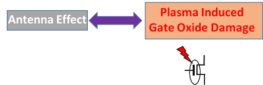
During the chip manufacturing process, a large conductor is connected to the gate oxide layer of the MOS tube. When ion etching is performed, the large conductor acts like an antenna, continuously collecting charges, causing the voltage on the conductor to become higher and higher, eventually breaking down the gate oxide layer of the MOS tube and causing the MOS tube to fail. This is the process antenna effect (PAE).
In the chip manufacturing process, the front-end process (FEOL) is first carried out, involving the manufacturing of all MOS transistors. Once the FEOL process is completed, the back-end process (BEOL) manufacturing begins, involving the manufacturing of metal interconnects. The antenna effect appears during the BEOL process.
During integrated circuit manufacturing, plasma etching processes are used to create metal interconnects. Plasma etching is a dry anisotropic etching process used for selective etching. The plasma contains high-energy ions and free radicals, which are collected by metal interconnects during metal etching. Figure 1 shows the MOS structure and the structure in which plasma is collected by interconnects.
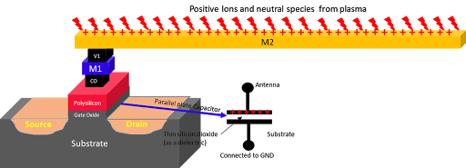 Figure 1 MOS structure and plasma etching
 The amount of charge accumulation depends on the surface area of the interconnect. These collected ions increase the potential of the interconnect and ultimately the gate if the interconnect is connected to a poly gate. As the gate potential increases, a leakage path may form through the gate oxide to the substrate to balance the additional charge accumulation on the gate. If the amount of accumulated charge is large, the leakage path through the gate oxide may destroy the gate oxide, causing permanent damage to the MOSFET, or create charge trapping in the gate oxide, which in turn can lead to many side effects such as early gate oxide destruction, mobility degradation, and threshold voltage shifts.
Gate oxide damage is primarily caused by plasma etching of metal interconnects, so this effect is also known as "plasma-induced gate oxide damage" or "antenna effect." The metal interconnect that collects the plasma (ions) and connects to the gate is basically called an antenna.
(1) Interconnect manufacturing process
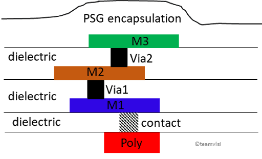
On the polysilicon, a layer of dielectric is deposited and then contact cut is performed. On the contacts, deposit Metal-1 and pattern and etch the excess metal, filling the entire area with dielectric. Before fabricating Metal-2, the pass-through media is cut and filled with pass-through media, and Metal-2 is then deposited on the pass-through media. Etch metal 2 again in the same way and fill it with dielectric. This process will be repeated multiple times depending on the number of metal layers. At the end of all metal processing, PSG packaging is performed as shown in the figure.
For each metal layer, through the corresponding via/contact, there are essentially three steps.
- deposition
- etching
- CMP
In the first step, metal is deposited, in the second step, unwanted metal areas are etched away, and in the third step, CMP (Chemical Mechanical Polishing) is performed.
Now let's talk more about the etching process. There are basically two etching processes, one is called wet etching with chemicals and the other is dry etching with gases. Dry etching provides fully anisotropic etching where the lateral etch rate is zero. The most popular plasma etching is a dry etching process, briefly described below.
(2) Plasma etching
A brief introduction to the plasma etching process will be given here to provide an understanding of the process. Plasma etching involves a high-velocity stream of plasma sprayed onto the sample with an appropriate gas mixture. The plasma source is called the etching species, which can be charged ions, neutral atoms, or free radicals. During the etching process, the plasma generates volatile etch products from chemical reactions between the target material and the reactive species generated by the plasma. The basic setup for plasma etching is shown below.
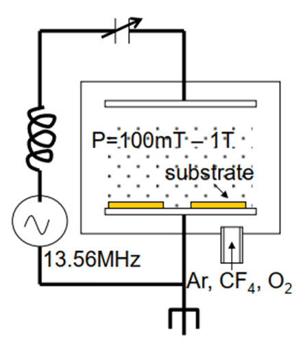 Figure 2 Plasma etching setup
 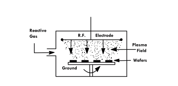 Figure 3 Plasma etching process setup in semiconductor manufacturing
 The top and bottom electrodes are equal in size and parallel. The bottom electrode holds the wafer and is connected to ground. Due to the application of radio frequency voltage and high voltage (P=100mT to 1T), a plasma is established between the two electrodes. High-energy electrons react with gas molecules and produce various reactive species, neutral species, and ions. Neutral species provide chemical etching, ions provide physical etching, and a combination of reactive species and ions provides ion-enhanced etching.
2 Conditions for the occurrence of antenna effect
① Occurs during the chip manufacturing process: does not occur during transportation, storage, and application.
② Occurs during ion etching: There are charged particles only during ion etching, and the suspended conductor will absorb these charged particles to generate voltage.
③ Occurs on the gate oxide layer: The gate oxide layer is a thin film sio2. When the suspended conductor of the gate absorbs a large number of charged particles, the gate potential is raised, and the gate oxide may eventually be broken down. The source and drain will not have an antenna effect, because there is no sio2 isolation layer on the source and drain, and they directly contact the metal layer. In addition, there are parasitic diodes on the source and drain, which can discharge the charges collected by the suspended conductors on the source and drain, thus not causing damage to the source and drain.
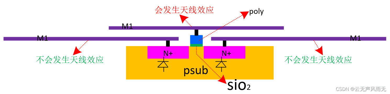
④ There must be a large conductor on the gate oxide: the conductor includes polysilicon poly layer and metal layer, because both poly and metal can conduct electricity, and large areas of poly and large areas of metal will cause antenna effects. You should be careful not to use poly to connect long wires in the layout. The antenna effect of poly can only be cut off, and it can be prevented by using metal connections. It is meaningless to add a leakage diode, because the diode needs to be connected to the electrode through metal, and finally it has to be connected to the poly through a via hole. The metal has not been made when etching the poly. At this time, the diode is not connected to the poly at all, and it cannot discharge the charge.
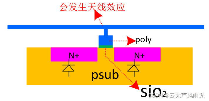
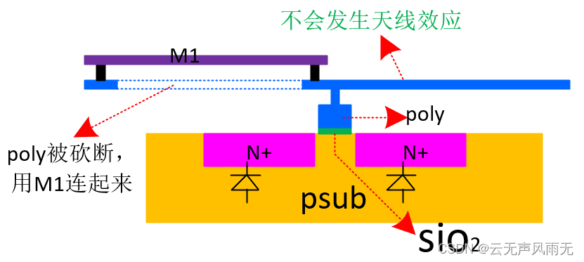
3 Evaluation conditions for producing antenna effects
Although the antenna effect occurs during the fabrication stage of the chip, especially during the plasma etching process, prevention mechanisms should be set in the physical design stage. The fabrication lab provides the antenna rules document, which must be inspected during the physical signoff phase, and the design should be cleaned according to the antenna rules. In DRC rules, the antenna ratio is generally used to determine whether antenna effects will occur. The antenna ratio is the ratio of the conductor area to the gate oxide area connected to the same point. Nets that violate antenna effect rules can be checked through DRC's antenna rule.
4 How to prevent antenna violations?
Before discussing prevention, let us review the root causes of the antenna effect and then understanding prevention techniques will become easy. The antenna effect is primarily caused by excessive charge accumulation on the metal interconnects connected to the transistor gates during plasma etching of the metal interconnects. The amount of charge accumulated depends on the area of the metal interconnect connected to the gate. Excessive accumulated charge is released through the thin gate oxide and causes permanent damage to the gate oxide.
Based on the above reasons for antenna violations, the following three methods can be used to prevent this problem. The first approach is to reduce charge accumulation by reducing the area of the metal interconnects connected to the transistor gates. The second method is to increase the gate area so that the ratio of (metal area)/(gate area) is less than the maximum allowed metal to gate area ratio. This can be achieved by connecting the floating gate to the relevant network. A third approach is to provide an alternative path for draining the charge accumulated on the transistor gate, i.e. adding an antenna diode.
Three basic techniques for preventing antenna violations are as follows:
- metal jump
- floating gate connection
- Antenna diode
Now it is important to understand the antenna rules and violations. We will return to this point after looking at the antenna rules.
(1) Antenna rules
The Process Design Kit (PDK) comes with some rule files. The antenna ruleset is part of the rules file. All rule sets must be checked before submission. Among antenna rules, the most common rule is antenna ratio.
- The antenna ratio is the ratio of the metal area connected to the gate to the total gate area.
- The antenna ratio is defined as follows:
- Antenna area / grid area < Maximum antenna ratio
Examples of antenna rule violations:
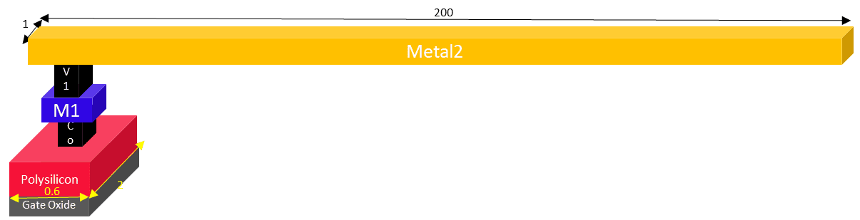
Consider the following three situations:
Case 1: Assume that the length of metal 2 is 200μm and the width is 1μm. As shown in the figure above, this metal wire is connected to the gate of a transistor. The transistor has a gate width of 2μm and a length of 0.6μm.
Therefore:
- Total metal area = 200×1 = 200μm^2
- Total gate area = 0.6×2 = 1.2μm^2
- Antenna ratio = 200/1.2 = 166.2
Case 2: Assume the same situation as case 1, but metal 2 is connected to 4 transistors instead of 1.
- Total metal area = 200×1 = 200μm^2
- Total gate area = 0.6×2×4 = 4.8μm^2
- Antenna ratio = 200/4.8 = 41.66
Case 3: Assume that metal 2 is divided into two sections, each section is 50μm, and connected through metal 3, as shown in the figure below. This connection is called metal hopping.
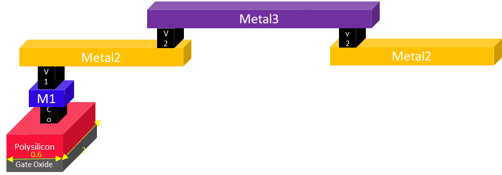
- Total metal 2 area = (50×1)×2 = 100μm^2
- Total gate area = 0.6×2 = 1.2μm^2
- Antenna ratio = 100/1.2 = 83.33
Assume that the antenna ratio is specified as 100. Therefore, among the above three cases, Case 1 violates the antenna rules, while Case 2 and Case 3 do not violate the antenna rules.
(2) How to fix antenna violations
The above example shows that if you increase the gate area by increasing the number of connected transistors, you will reduce the antenna ratio. Another way to fix antenna violations is by reducing the antenna area, i.e. disconnecting and inserting jumpers between the metal. Therefore, we can reduce the antenna ratio in two ways:
- Reduce antenna area - insert jumpers or metal jumpers
- Increase gate area - insert dummy transistors
Antenna inspection (physical verification)
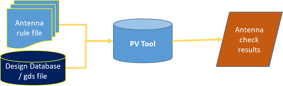
- The antenna check verifies that the layout complies with the antenna rules in the rules file. Before submission, there are many other checks that need to be performed, such as DRC, ERC, LVS, etc. These are collectively called the physical verification of the layout.
- Physical verification tools (e.g. Caliber, Assura, IC Validator) validate antenna rules against all layers where the antenna rules apply.
- Antenna rules are highly dependent on the process node.
Antenna violation repair measures
1. Insert jumpers or metal jumpers

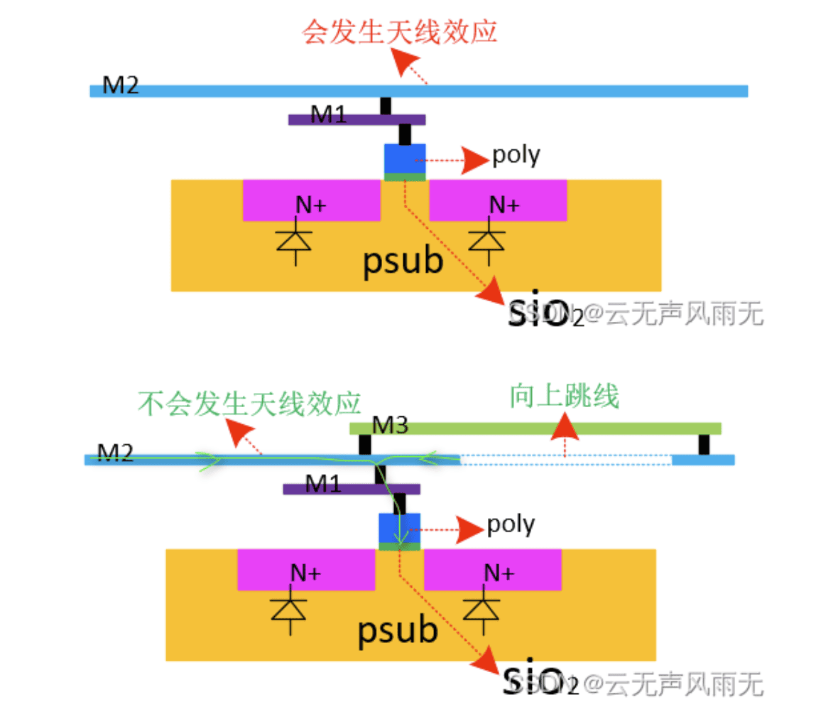
Cut off the long traces and jump up the wires. When this layer of metal collects charges, the upper layer of metal has not yet been done, which is equivalent to reducing the area of the antenna and preventing the antenna effect. This approach increases routing complexity and affects timing when dealing with high-speed signals.
special attention: The downward jumper cannot solve the antenna effect. It should be because when the metal of this layer collects the charge, the lower metal is already ready and connects the cut metal of the layer together, which does not reduce the area of the antenna, so it cannot prevent the antenna effect.
2. Insert dummy transistor

As shown in the figure above, the effective gate area can be increased by inserting dummy transistors. This will reduce the antenna ratio and help meet antenna regulations. In a practical case we could add a floating reverser/buffer. We connect the input of the buffer/inverter to the relevant network and keep the output floating. This will increase the effective gate area and help resolve antenna violations. In essence, it reduces the antenna area, but it will increase the signal delay and is not suitable for circuits with relatively high timing requirements. Moreover, this method does not work with analog signals, only with digital signals.
3. Insert reverse diode
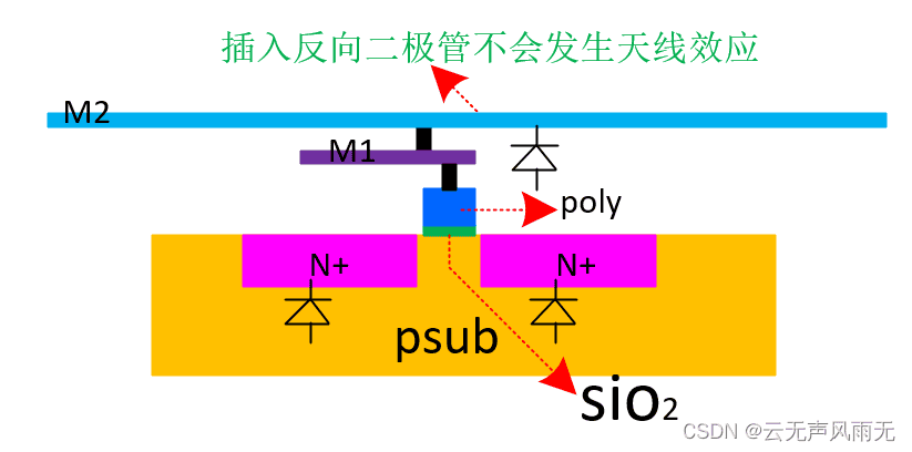
When the chip is working normally, the diode is in a reverse biased state and will not affect the circuit function. When the antenna effect occurs, the reverse-biased diode preferentially breaks down the MOS and releases the charges collected on the antenna to protect the MOS tube. Generally, stdcell will provide this kind of anti-antenna diode device, which can be added to the schematic and layout. If not, you can draw one by yourself, or call a diode in the pdk. What you need to pay attention to is to ensure that the diode is in a reverse biased state during normal operation, or problems such as leakage or abnormal function may occur. Using this method may increase the chip area and needs to be considered comprehensively.
thank you
https://teamvlsi.com/2020/05/latch-up-prevention-in-cmos-design.html
https://zhuanlan.zhihu.com/p/660374839
https://blog.csdn.net/al20093064/article/details/133715942
https://teamvlsi.com/2020/06/antenna-prevention-techniques-in-vlsi.html