According to research from Collett International Research Inc., about one in five chips fails due to signal integrity issues. This data is no joke! This brings us to an in-depth discussion of an extremely important topic in VLSI design - signal integrity and crosstalk.
Signal integrity:
First, let’s clarify what signal integrity is. Signals are essentially information transmitted in the form of waves/pulses that are used to enable communication between different points. For example, a signal in digital form can be state 1 (high level) or state 0 (low level), just like language in a binary world. As shown below.

Figure 1 Digital signal
By definition, integrity means “complete or unimpaired.” Or we can say, maintaining the actual form of anything over time without distortion. Therefore, signal integrity can be defined as the overall reproduction of a signal without any distortion in quality when transmitted from one point to another. Or from a broader perspective, we can say that signal integrity is the ability of an electrical signal to reliably carry information and resist high-frequency electromagnetic interference from nearby signals.
In the topic of signal integrity, we will encounter three major elements: signal, chip, and transmission channel. The signal is the subject being transmitted, and understanding the characteristics of the signal is the primary task; the chip is divided into a driver chip and a receiving chip, and signal integrity engineers need to ensure that the signal can be transmitted correctly between the two; the transmission channel is the "road" the signal takes, and signal integrity engineers are required to "build roads" and "build bridges" to ensure that the signal is unimpeded.
- Signal: It is the subject being transmitted. We must first understand and be familiar with the characteristics of the signal.
- Chip: It is divided into a driver chip and a receiving chip. The signal integrity engineer is to realize the correct transmission of signals between the driving chip and the receiving chip.
- Transmission channel: It is the medium for transmitting signals and the "road" that the signal takes. How to achieve correct transmission of signals? That requires signal integrity engineers to "build roads" and "build bridges" for signals.
Signal integrity solves two problems in digital design:
- Timing of the signal - Does the signal arrive at its destination at the intended time?
- Quality of signal - When the signal arrives, is it of good quality?
In high-speed digital design, "timing" is very important.
Therefore, the goal of signal integrity is to ensure reliable high-speed data transmission from one point to another within the chip through metal lines. As data rates increase and technology nodes decrease, maintaining signal integrity is a huge challenge. Simply put, signal integrity is high if the signal travels through the network without any distortion; signal integrity is low if there is a lot of noise added/distortion occurring/delay occurring.
In addition to the key issues mentioned above, signal integrity is often affected by a variety of other factors. Crosstalk is one of them. When different signals interfere with each other, it may cause signal distortion and delay. In addition, ground bounce is also a common problem. When a large amount of current changes on the ground line, it may cause the ground potential to fluctuate, thus affecting signal transmission. There are also IR voltage reduction, antenna effect, electromigration and so on.
What is crosstalk?
Crosstalk can be defined as a phenomenon in which logic transmitted in one network has an undesirable effect on its neighboring networks. In other words, the switching of signals in one network can interfere with adjacent networks. This is known as crosstalk. When a signal switches, it may affect the voltage waveform of adjacent networks. The switching network is often called the "aggressor" and the affected network is called the "victim." Figure 2 shows how a typical aggressor and victim network are arranged.
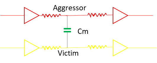
Figure 2 Aggressor and victim network
Crosstalk is a very serious effect, especially inlower technology nodeandhigh speed circuit, it could beChip failureOne of the main reasons. In the next section, we will discuss the crosstalk mechanism in VLSI designs.
crosstalk mechanism
Crosstalk occurs through two mechanisms:
- Induced crosstalk
- electrostatic crosstalk
Induced crosstalk occurs due to the phenomenon of mutual inductance between two networks. Changing currents in a network produce changing magnetic fields around the network. Changing magnetic fields can both radiate energy by emitting radio frequency waves and couple with adjacent networks. This coupling of magnetic fields is called inductive crosstalk.
Electrostatic crosstalk occurs due to mutual capacitance between two networks. Voltage in a network creates an electric field around it. If the electric field changes, it can either radiate radio waves or capacitively couple to adjacent networks. This coupling of electric fields is called electrostatic crosstalk.
Of the two mechanisms explained here, the electrostatic crosstalk mechanism is more significant and problematic than inductive crosstalk.
Parasitic capacitance associated with interconnects
The main cause of crosstalk is the capacitance between interconnects. Therefore, in this section we will investigate the various capacitances associated with metal interconnects. Figure 3 shows the various parasitic capacitances formed inside the ASIC (click on the image for a better view).
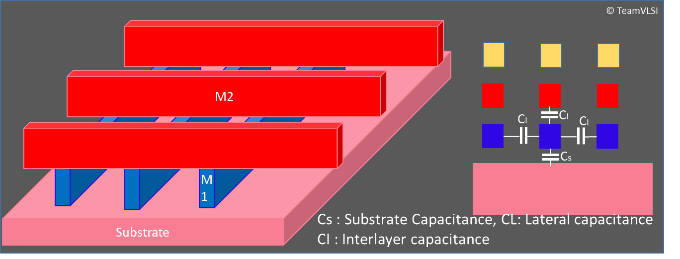
Figure 3 Various capacitances associated with interconnects
After the FEOL (front end of line) fabrication is completed, a thick SiO2 insulating layer is deposited over the entire substrate before the metal-1 (M1) layer is fabricated. The insulating layer between M1 and the substrate acts as a medium and forms a capacitance between M1 and the substrate, which is called substrate capacitance (cs). M1 is machined and the unnecessary metal areas are etched away before the empty areas are filled with SiO2. Therefore, a parasitic capacitance is formed between two adjacent M1 meshes (same metal layer), called lateral capacitance (CL). Make an M2 layer on top of M1, then the SiO2 layer. Therefore, interlayer capacitance (CI) is formed between any two adjacent metal layers. Interlayer capacitance can not only form between interconnected metals, but also between metals that are far apart, such as M2-M4 or M2-M5. The value of all these capacitors depends on two factors: the common area and the gap between them. These capacitances are directly proportional to the common area between them and inversely proportional to the gap between them.
thank you
[1] https://teamvlsi.com/2020/06/signal-integrity-and-crosstalk-in-vlsi.html
[2] https://blog.csdn.net/qq_29476769/article/details/122854047
[3] https://blog.csdn.net/qq_29476769/article/details/122933743
[4] https://blog.csdn.net/qq_29476769/article/details/122953752