In a previous article, we have discussed signal integrity, crosstalk, crosstalk mechanisms, and parasitic capacitance associated with interconnects. In this article, we will discuss the effects of crosstalk. Crosstalk has two main effects:
- Crosstalk glitches or crosstalk noise
- Crosstalk delta delay or crosstalk delay
crosstalk glitch
To explain crosstalk glitches, we will consider the following two scenarios. There may be many similar situations.
Scenario 1: The intruding network switches from low level to high level, and the victim network remains at a constant low level.
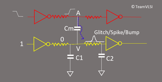
Figure 1 Crosstalk glitch (rising)
In this case, the aggressor network switches from logic 0 to logic 1 and the victim network remains at a constant zero, as shown in Figure 1. Now consider node A, node V, mutual capacitance Cm, and the path from A to V. As node A switches from low level to high level, a potential difference is generated between the mutual capacitances, and the mutual capacitance Cm begins to charge. During this process, due to the leakage characteristics of mutual capacitance, some leakage current will begin to flow from node A to node V through mutual capacitance Cm, which will increase the potential of node V, thereby generating a rising spike or burr on the victim network, as shown in Figure 1. The size of this voltage or the height of the glitch depends on various factors that will be discussed later.
So every time one net switches from low to high while another adjacent net should stay constant low, it will be affected by the switched net and create a glitch on it. Now let us discuss case two which is similar to case one.
Scenario 2: The intruding network switches from high level to low level, and the victim network remains at a constant high level.
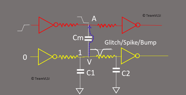
Figure 2 Crosstalk glitch (drop)
In this case, the aggressor network switches from logic 1 to logic 0, while the victim network remains constant high, as shown in Figure 2. Now consider node A, node V, mutual capacitance Cm, and the path from V to A. As node A switches from high level to low level, a potential difference is generated between the mutual capacitances, and the mutual capacitance Cm begins to charge from node V to node A. During this process, due to the leakage characteristics of the mutual capacitance, some leakage current will begin to flow from node V to node A through the mutual capacitance Cm, which will reduce the potential of node V, thereby generating a falling spike or glitch on the victim network, as shown in Figure 2.
So, in case one and two, we see that if one network is switching and another adjacent network is maintaining constant logic, and there is mutual capacitance between them, then the other network can be affected and can have a sudden up or down bump or spike on it. Such spikes on the victim network are called crosstalk glitches or crosstalk noise. Figure 3 shows the situation where a rising glitch or a falling glitch occurs.
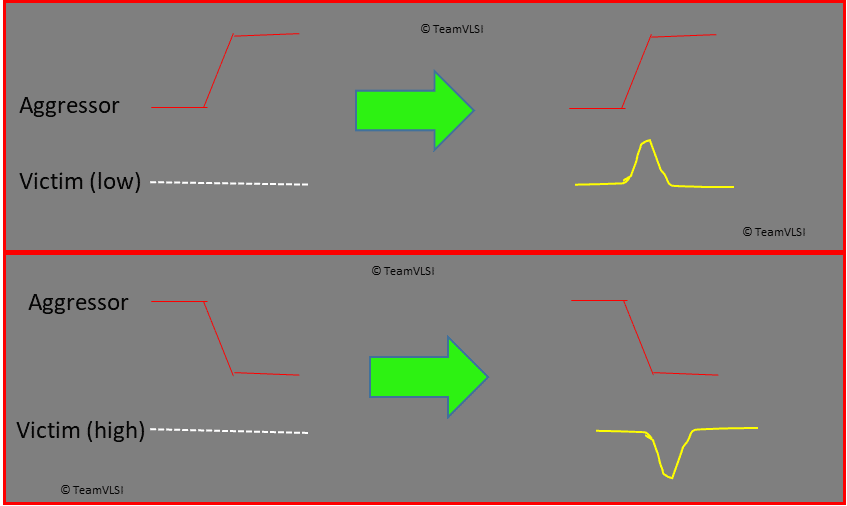
Figure 3 Rising and falling glitches in crosstalk
Effect of crosstalk glitches
Is every burr unsafe? The answer depends on the height of the glitch and the logical connectivity of the victim network. Such glitches are considered safe glitches if their height is within the Noise Protection Low (NML) range. If the height of the glitch exceeds the noise protection high (NMH), such a glitch is considered a potentially unsafe glitch. If the height of the glitch is between NMH and NML, this is an unpredictable situation. Figure 4 shows the CMOS inverter transfer characteristics and noise protection range.
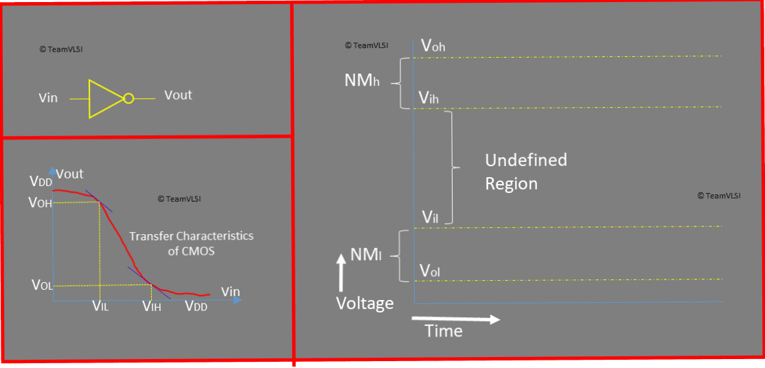
Figure 4 CMOS transmission characteristics and noise protection range
As technology nodes shrink, supply voltages also decrease. At lower supply voltages, the noise protection range will be smaller. If the noise protection range is smaller, potentially unsafe glitches are more likely to occur. Figure 5 will help understand this fact.
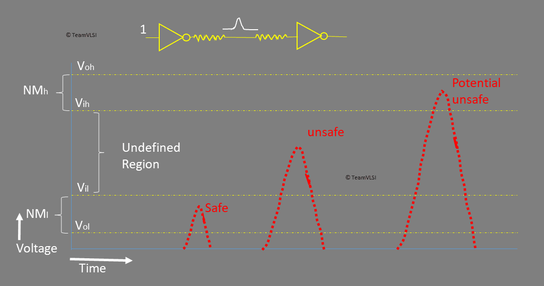
Figure 5 Safe and unsafe burrs based on burr height
Figure 5 shows safe and unsafe burrs based on burr height. The security glitch has no effect on the victim network's next logic, and the victim network's logic will be treated as the correct logic. But in other cases, due to the impact of glitches, the logic of the victim network may be perceived as faulty logic, thereby propagating erroneous data and possibly causing chip failure. Typically, a memory's reset pin is a constant logic, and if the pin's network experiences unsafe crosstalk glitches, the memory may be reset. Many other situations can occur that cause chip failure due to unsafe glitches.
But there are some cases where crosstalk glitches have no effect. For example, consider a two-input AND gate with one input connected to a constant 0 and crosstalk occurring at the other input. Therefore, regardless of the effects of crosstalk, the output is always zero. A similar situation exists for many combinational logics where crosstalk has no effect. Likewise, if the glitch height is within the low noise protection range, this is also the case.
Crosstalk glitch height
Whether a crosstalk glitch is safe or unsafe depends on the height of the crosstalk glitch and the logic pin to which the victim network is connected. So, let’s investigate what factors crosstalk glitch height depends on. Crosstalk glitch height basically depends on three factors:
- coupling capacitor
- Intrusion drive strength
- Victimization Drive Strength
The closer the networks are, the greater the coupling capacitance. The larger the capacitance, the greater the height of the glitch. The drive strength of the intruder network and the victim drive also affects the height of the glitch. High drive intensity on the intruder network will have a greater impact on the victim network. If the victim network is driven with high strength, it is not easy to change its value, which means the impact of crosstalk will be smaller.
That’s all about crosstalk glitches or crosstalk noise, now let’s turn to the second effect, which is crosstalk delta delay or crosstalk delay.
crosstalk delay
Crosstalk delay occurs when the aggressor and victim networks switch simultaneously. It will have an impact on the setup and hold times of the design. Crosstalk delays can cause setup and hold time violations. Therefore, it is important to perform a crosstalk delay analysis and correct the timing considering the impact of crosstalk. Crosstalk may increase or decrease a unit's latency, depending on the switching direction of the aggressor and victim networks. We will consider two cases, one where both networks are switching simultaneously in the same direction (high to low or low to high), and one where two networks are switching in opposite directions, and analyze the impact of crosstalk delay.
Scenario 3: The intruder network and the victim network switch in opposite directions
Let us consider the intruder network switching logically from low to high and the victim network switching logically from high to low (in the opposite direction), as shown in Figure 6.
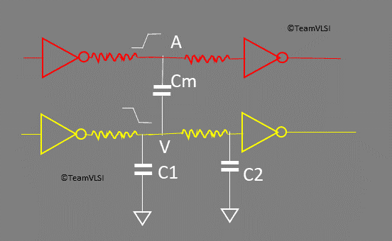
Figure 6 Crosstalk delay due to opposite direction switching
When node A starts switching from low to high, node V starts switching from high to low at the same time. During half of the conversion process, there is a potential difference from node A to node V. There is a coupling capacitance between node A and node V, so the aggressor node will try to boost the victim node. This will affect the victim node's smooth transition from high to low and will create a bump after half of the transitions, causing the victim network's transition time to increase. Figure 7 shows the transformation process of the network. After crosstalk, the unit's delay will increase by Δ, and the new delay is D + Δ.
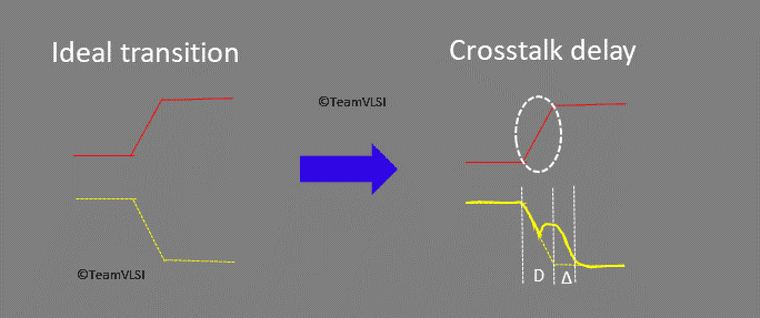
Figure 7 Crosstalk delay (increased)
Scenario 4: The intruder network and the victim network switch in the same direction
Let us consider that the intruder network switches from low to high logic and the victim network also switches from low to high logic (same direction) as shown in Figure 8.
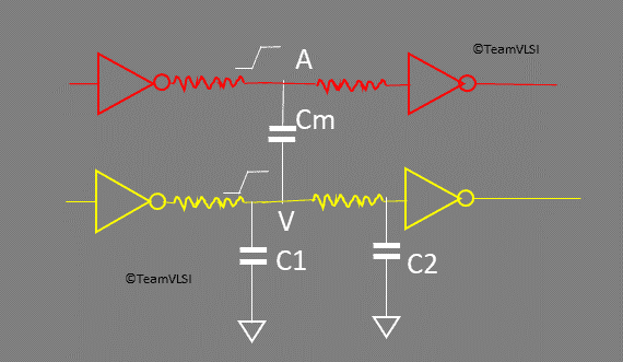
Figure 8 Crosstalk delay due to switching in the same direction
When node A starts switching from low to high, node V also starts switching from low to high. Assuming that the intrusion network has high driving strength and fast switching, a potential difference will be generated from node A to node V after half of the switching process. There is a coupling capacitance between node A and node V, so the aggressor node will try to boost the victim node quickly. This will affect the victim node's smooth transition from low to high and create a bump after half of the transitions, resulting in reduced transition time for the victim network. Figure 9 shows the transformation process of the network. After crosstalk, the unit's delay will be reduced by Δ, and the new delay is (D - Δ).
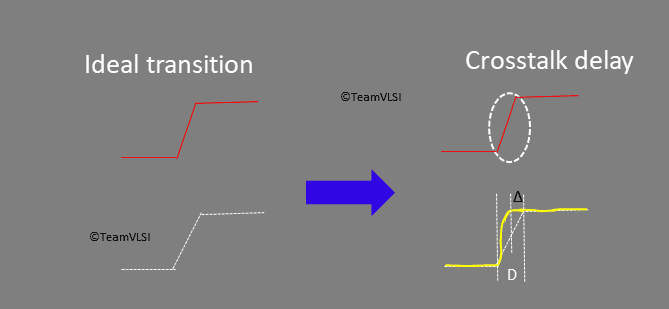
Figure 9 Crosstalk delay (reduction)
Effect of crosstalk delay
Crosstalk delays have various effects on the timing of your design. It can unbalance a balanced clock tree, potentially violating setup and hold times. In this section, we discuss some of these effects.
Impact on the clock tree:
Crosstalk can unbalance a balanced clock tree. Crosstalk delay may increase or decrease the delay of clock buffers in the clock path, and a balanced clock tree may become unbalanced, as shown in Figure 10.
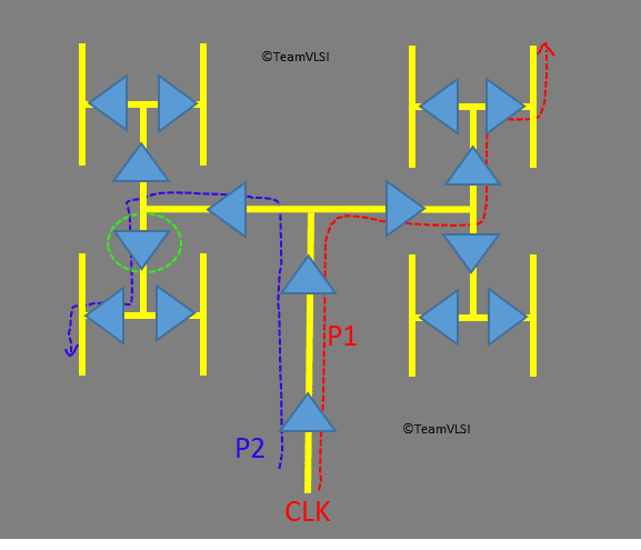
Figure 10 The impact of crosstalk delay on the clock tree
Assume that the delay of path P1 is L1 and the delay of path P2 is L2. If the clock tree is balanced, then L1 must equal L2. Now assume that crosstalk delay occurs and affects one of the clock buffers in clock path P2. So now L1 is no longer equal to L2, and the clock tree is no longer balanced. Here, we only consider one clock buffer being affected by crosstalk delay, but in reality there may be multiple effects.
Effect on setup time and hold time:
Crosstalk delays may violate the setup time. Figure 11 shows the data path, transmit clock path, and capture clock path.
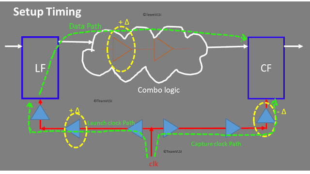
Figure 11 Effect of crosstalk delay on setup time
For setup time, the data should arrive at the catcher before the time required by the catcher. Therefore, if the delay in the data path or transmit clock path increases, it may cause a setup violation. Setup violations may also result if the latency on the capture clock path is reduced. The effects of these crosstalk delays must be considered and time corrected.
Hold time may be violated due to crosstalk delays. Figure 12 explains the situation where a hold time violation occurs due to crosstalk delay.
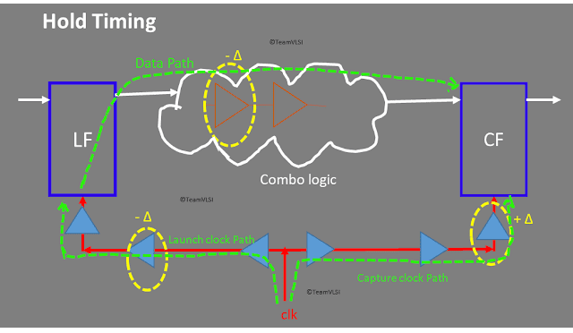
Figure 12 Effect of crosstalk delay on hold time
Hold time violations can result if the delay of any cell in the data path and transmit clock path is reduced, or if the delay of a cell in the capture clock path is increased due to crosstalk delays. These situations must be taken into account and the timing corrected.
thank you
[1]https://teamvlsi.com/2020/06/crosstalk-noise-and-crosstalk-delay-effects-of-crosstalk.html