1. Problem background
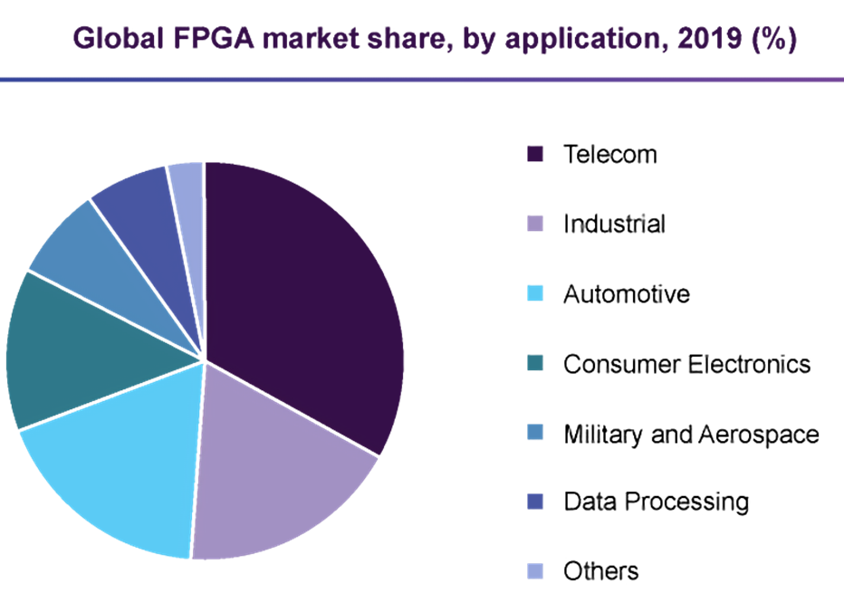
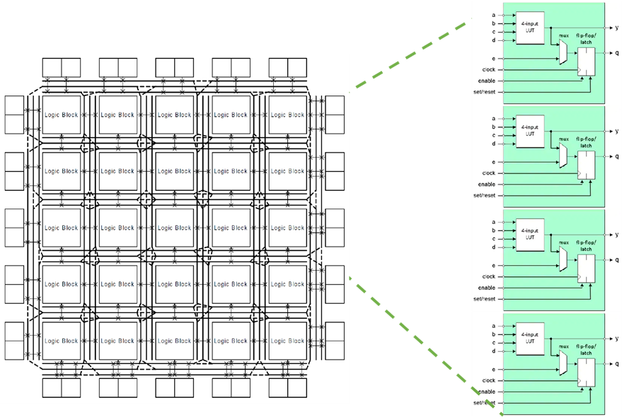
With the increasing complexity of chip design and the continuous development of advanced technology, as shown in Figure 1, FPGA (Field Programmable Gate Array) is increasingly used in chip prototype verification and embedded systems. FPGA process mapping is an essential process for mapping logic circuits to programmable logic lookup tables (LUTs), which is crucial to the performance, power consumption, and area (PPA) of FPGA designs. Figure 2 is the basic structure of FPGA.
However, as design sizes increase and performance requirements increase, traditional process mapping algorithms face challenges. These algorithms may have shortcomings in dealing with large search spaces, optimization of timing constraints, improvement of resource utilization, and reduction of power consumption. In order to improve the performance and resource utilization of FPGA design, it is necessary to optimize the FPGA process mapping algorithm.
2. Problem description
2.1 Description
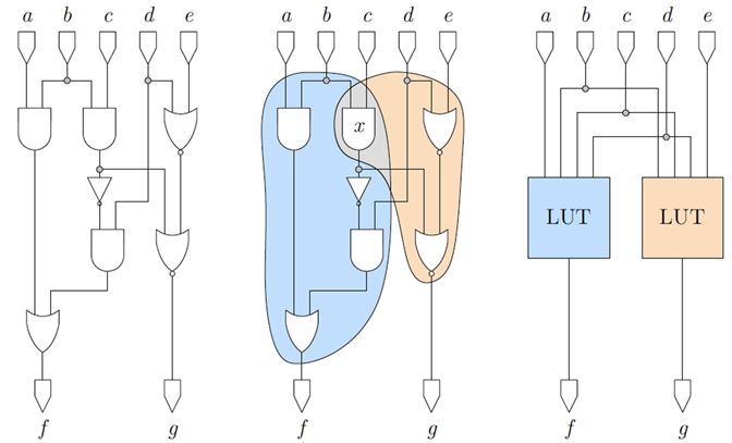
Figure 3 shows an overview of a traditional FPGA process mapping algorithm. The main process is to enumerate CUT groups for each node of the original circuit, then sort the CUT groups of each node by characteristics such as area and depth, and then select the optimal CUT on each node to achieve coverage of the entire circuit area. From the perspective of the process of the traditional algorithm, there are still many areas that can be further improved and optimized.
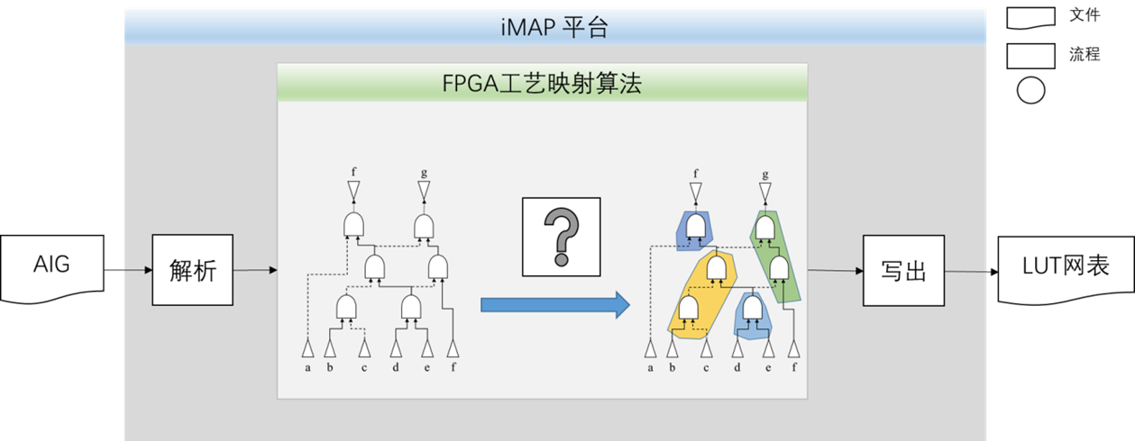
As shown in Figure 4, this issue focuses on the design of process mapping algorithm based on intelligent CUT selection. The algorithm will utilize intelligent screening and priority cutting techniques to reduce unnecessary search space and improve the efficiency of process mapping. By analyzing the structure and characteristics of the logic circuit, the algorithm can intelligently select the optimal cut set (Cut Set) as a candidate mapping target. At the same time, the algorithm will also optimize the selection order of cut sets to further reduce the search space and improve the mapping effect.
The goal of this problem is to design an efficient intelligent screening-first-cut process mapping algorithm that can provide excellent PPA performance in large-scale and complex FPGA designs. The algorithm needs to consider multiple factors, such as the size of the logic circuit, timing requirements, resource constraints, and power consumption constraints. The design of the algorithm will make full use of intelligent screening and priority cutting technology, combined with advanced optimization methods, to achieve efficient process mapping and optimization.
2.2 Problem case
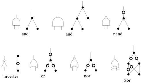
The input file of each case is a combinational logic circuit in AIG (And-Inverter Graph) format. Each basic gate in the AIG circuit is an AND gate or a NOT gate, as shown in Figure 5. The AND gate and NOT gate are logically complete groups that can represent all other basic gate units.
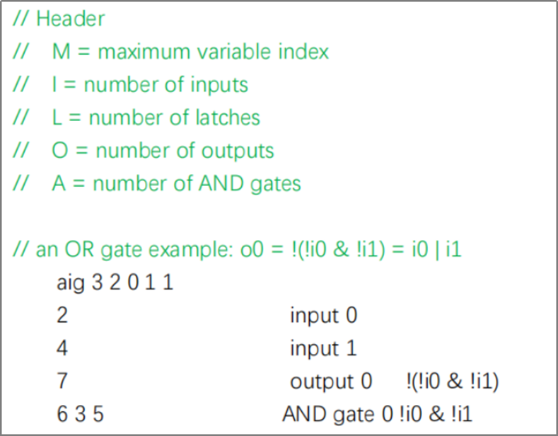
A typical input file is shown in Figure 5 (this question only targets the combinational logic netlist, so the third item L is always 0):
2.3 Output requirements
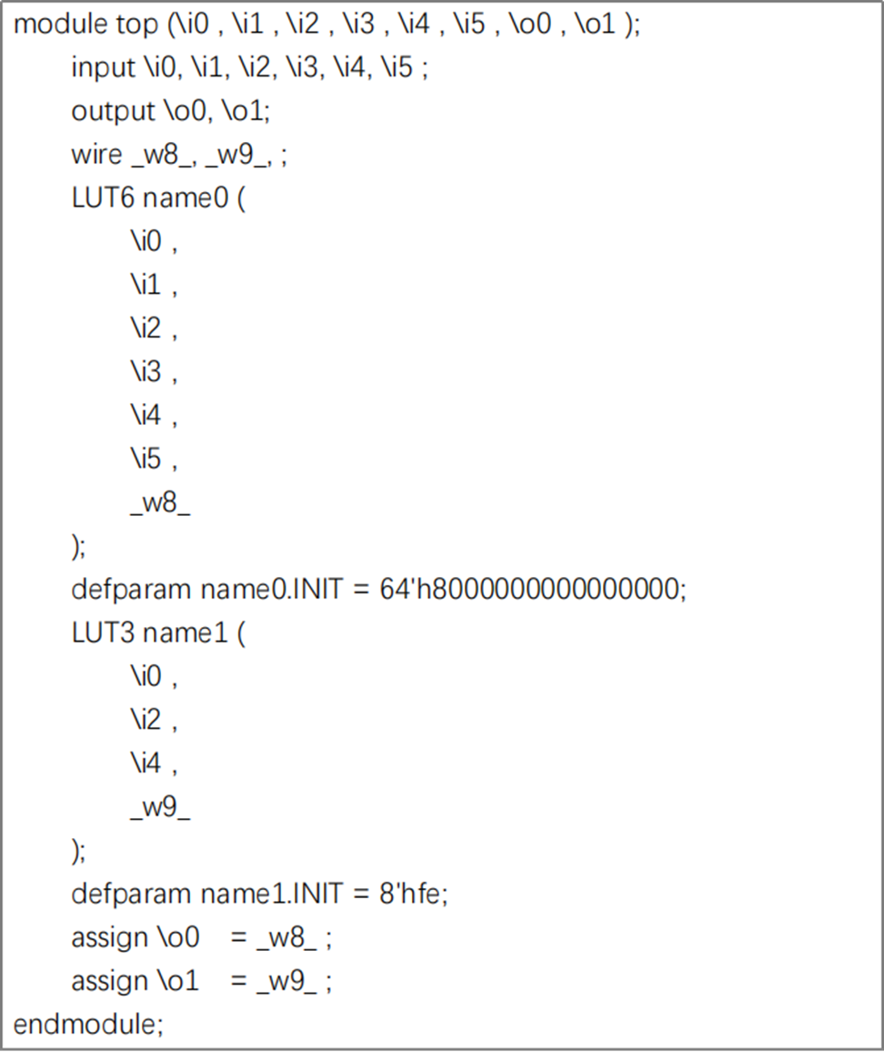
The output file is a netlist composed of LUTs. A K-input LUT is essentially a single-output RAM with a K-bit address, which can implement any K-input Boolean logic by storing a truth table.
A typical output file is shown in Figure 7, where o0 = i0&i1&i2&i3&i4&i5; o1 = i0|i2|i4.
2.4 Competition environment
(1) Operating environment
Operating system: linux system;
Hardware environment: 64-bit x86 CPU, 128GB running memory, 1TB hard drive, NVIDIA-GPU;
Software environment: gcc7.5.0, g++7.5.0, glibc2.27, python3.7, cuda-driver.
(2) Reference tools
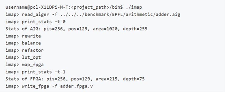
As shown in Figure 8, iMAP supports reading and writing of “.aig” files and writing of FPGA netlists. For participating teams, they only need to pay attention to the algorithm of the FPGA process mapping link.
3. Scoring criteria
(1) Necessary requirements: Pass the equivalence check. Ensure that the output FPGA netlist is logically equivalent to the original input AIG, otherwise this question will be scored 0 points.
(2) Weighted score: cost=50%*runtime+30%*delay + 20%*area. The lower the cost, the better the result quality, and the higher the score of the corresponding case.