logical synthesis RTL level circuit design (.v file), next chapterPhysical design of back-end place and route, the dividing line between the front and back ends, its goal is to convert circuits described at the RTL level into circuits described by the gate-level netlist based on a specific process library, and use SDC constraints to reflect PAP (performance, area, power consumption).
Design Compiler, referred to as DC, is the core tool used by Synopsys for synthesis. It can easily convert circuits described in HDL language into gate-level netlists based on process libraries.
Logic synthesis is a design method that uses Software methods to design hardware, and then leaves the work of gate-level circuit implementation and optimization to synthesis tools. It is based on the requirements of a system's logical function and performance, and with the support of a unit library containing many logical components with known structures, functions, and performances, to find the best implementation plan for a logical network structure. That is, under the conditions of meeting the constraints of the function, speed and area of the designed circuit, the behavioral level description is converted into the connections of the unit circuits in the specified technology library.
1 DC design object
During the synthesis process, DC will divide the circuit into different processing objects, which are calledDesign Objects, specifically as follows:
Design: The object to be synthesized.
Port: The outermost input and output ports of the entire Design.
Clock: The pin or port of the clock signal source. (Digital circuits use clock-based synchronous circuits. Any problems with the clock will have an important impact on the circuit, soBe sure to handle the clock port separately)
Cell: An instance of a subdesign contained in a design, also called an instance. (instantiated module)
Reference: The pointed design prototype, that is, the instance for which the unit is a reference. (instantiated prototype)
Pin: The pin of the cell itself.
Net: Internal connections, connections between ports and pins and between pins.
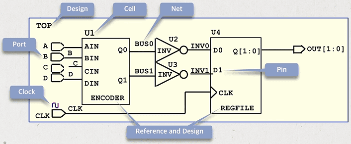
Figure 1 Schematic diagram
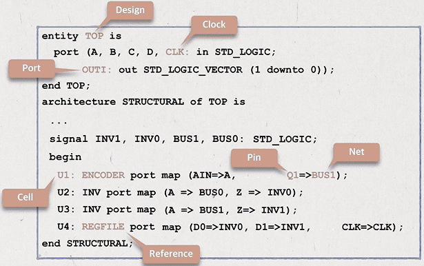
Figure 2 VHDL
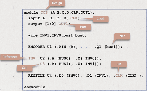
Figure 3 Verilog
It should be noted that design objects will have problems with the same name, as follows:
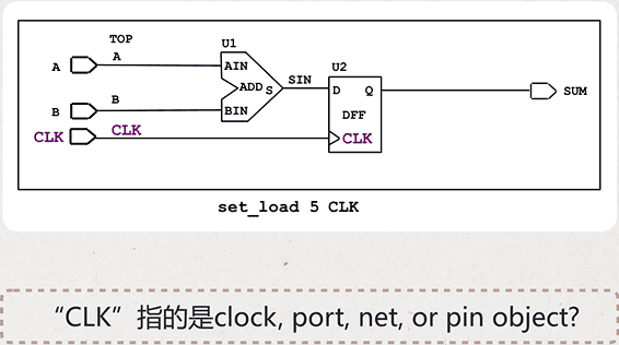
Adding constraints to different design objects will bring different results. The instructions in the above example do not clearly indicate which design object it is. Different versions of DC may handle design objects with the same name differently. You can use the get_* command to specify the design object (this command returns the object in the current design), such as set_1oad5[get_nets sum], which returns the one named sum among the nets type design objects.
2 DC working principle
To some extent, timing closure is an important goal of logic synthesis, and imposing timing-related constraints is an important step in synthesis (SDC file). DC has an embedded static timing analysis engine, Design Time,Complete design optimization and mapping based on timing constraints, making subsequent timing constraint settings more realistic.
In logic synthesis, there is an internal static timing analysis engine that divides the entire circuit into different timing paths. The starting point of the path is input port 、clock, the end point is Register D end, output port。
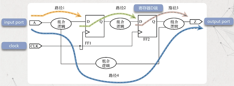
Based on static timing analysis, logic synthesis will have two indicators:Setup timeandhold time. [For details, you can learn the basic knowledge of STA in Part 5]
In the synthesis process, DC usesWhen maximizing the buildTime is the focus. If the build time does not meet the requirements, you can only iterate again and re-synthesize with the illegal path as the optimization goal; if the holding time does not meet the requirements, you tend to postpone the correction until after the layout.
DC is optimized for worst-case critical timing paths. Adopt the so-calledmaxmin algorithm, taking the maximum delay for the data path and taking the minimum delay for the clock path does not violate the setup time constraint; taking the minimum delay for the data path and taking the maximum delay for the clock path does not violate the hold time constraint.
This is a comprehensive strategy of DC, specifically the method of imposing timing constraints and the method of correcting time violations.
3 DC three stages
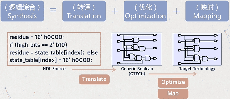
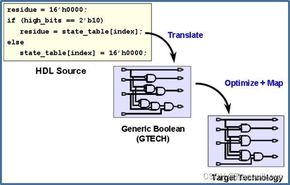
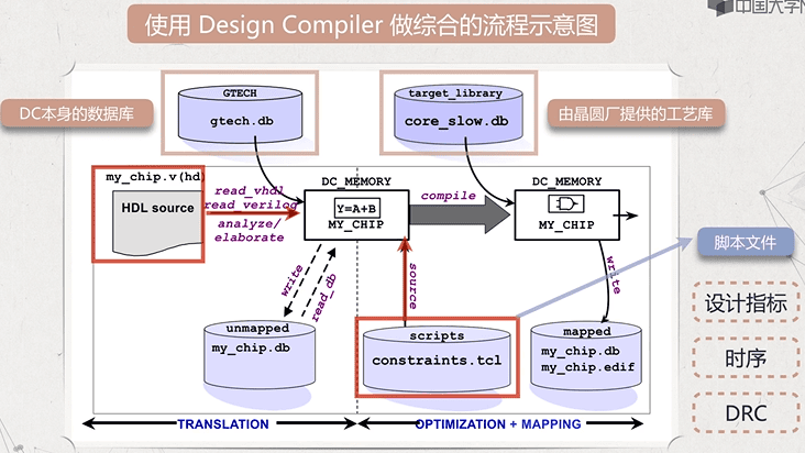
Translation: Convert HDL code into DC's internal database (GTECH library), which has nothing to do with technology;
Optimization: Optimize the circuit according to the design goals (frequency, area, power consumption) (independent of the process, using Boolean transformation or algebraic transformation technology), including structural optimization (Architectural level synthsis), logic optimization (Logic level or GTECH optimization) and gate-level optimization (Gate-level or Mapping optimization)
Mapping: Select appropriate logic units (including combinational logic and sequential logic) in the target library to generate the designed gate-level circuit
(Mapping is to map the general netlist GTECH library components to the gate-level standard units in the target library, such as registers, AND gates, OR gates, etc. The circuit netlist at this time contains relevant process parameters, such as netlist (V file), delay information (SDF file), YD information (SDC file), etc. The ddc file will contain the information of the above files.)
At this time, the optimization and mapping related to the process library and process parameters are carried out at the same time. There is no order of execution steps in translation and optimization, so the synthesis is aselection process。
GTECH (aeneric technology) netlist is a general netlist. Compared with process netlist, GTECH netlistNo specific process information, refers to the logic gate unit it uses is a symbol, including general logic gates (such as AND or NOT, flip-flops, etc.) and general operators (addition, subtraction, multiplication, division, shift, comparison, selection, etc.),GTECH netlists contain only logic functions, but can model power, latency, and area.
Taking the 16-to-1 multiplexer (MUX) as an example, the GTECH netlist represents it as a 16 x1 MUX with 16 inputs, 4 input selections, and 1 output; while the process netlist may represent it as a cascade of multiple 4x1MUXs based on the process library information.
4 DC file management
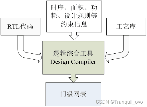
Design Compier reads the RTL code of the design and completes the conversion of the RTL-level circuit to the gate-level netlist on the target process library based on various constraints imposed by the user. The contents of its input and output files are as follows:
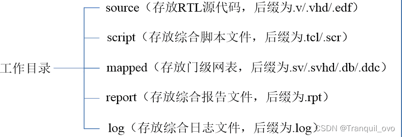
In order to facilitate the management of input and output files, the following Contents structure is usually established according to the file content under the working Contents to store the corresponding files.
5 DC basic process
Read library files (including target libraries, link libraries, symbol libraries, etc.)
Add timing constraints and design rule constraints (environmental constraints, area constraints, timing constraints, etc.)
Comprehensive RTL design (convert RTL code into a gate-level netlist represented in standard cells)
Analyze results
Export design data
6 DC library files
Several library files used by DC during operation are as follows:
- target library target library
- link library link library.
- symbol library symbol library
- arithmetic operation library synthetic library
target library
(The designer wants the DC to infer and ultimately map the process library corresponding to the logic unit on it.)
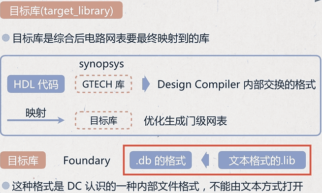
The read HDL code is first converted into the format exchanged within Design Compier by synopsys' own GTECH library, and then mapped to the process library and optimized to generate a gate-level netlist.
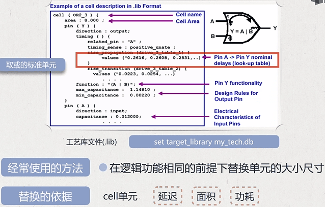
The target library is provided by the wafer factory. The format is .b, which is the internal format of DC and is unreadable. It can be converted from the text-readable .1ib format. The target library contains the behavior (logic function), pins, area and timing information of each gate-level unit (some process libraries also have power consumption parameters). During synthesis, DC calculates the path delay based on the delay information of the unit circuit given in the target library. And select the appropriate unit to optimize the circuit according to the delay, area and driving capability of each unit.
An example of a process library (Japanese standard library) is as follows. A common method of DC optimization is to replace the size of the unit under the premise of the same logical function. The replacement is based on various information contained in the process library.
link library
(Explain the reference of leaf units and sub-designs of the netlist. Each unit and design must find its reference in the link library to ensure the integrity of the design. Generally, the link library includes the target library PAD process library, ROM/RAM and other macro unit libraries, as well as DC design files read into the memory. At the same time, the library can also contain old process libraries that have completed remapping between different processes.)
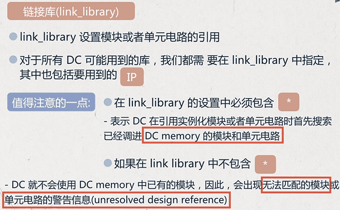
Normally,Link library corresponding IP, such as purchased paid IP, storage, IO, PAD, etc. The target library refers more to the standard unit, so the two may be the same or different. We must specify this in detail.
When setting the link library, pay attention to setting the search path as follows:
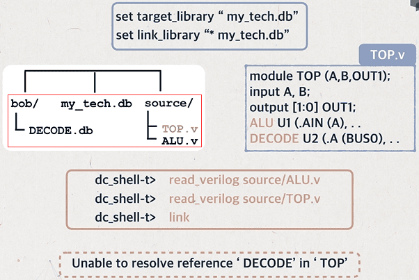
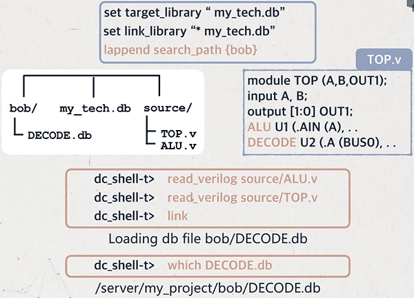
As shown in the figure above, in such a Contents situation, although 1ink_1ibrary is set, DC reports an error when 1ink is used, and the DECODEIP module referenced in ToP.v cannot be found. This is because the search path is not set and the DC cannot find the file. This also means that 1ink_1ibrary looks for relevant references under the Contents of the running DC by default. To enable the DECODE in the above example to be found, the search path needs to be set. As shown below:
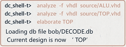
Files can also be read using the analyze & elabroate command, as follows:
symbol library
(The symbolic representation of the technology library components is used to graphically display the comprehensive gate-level netlist; if only the command line interface is used, the library does not need to be specified.)
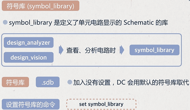
synthetic library
(Synthesis library, which contains proven, synthesizable, process-independent IP, also known asDesignWare. dw_foundation.sldb is the DesignWare library provided by Synopsys. It contains basic arithmetic operation logic, control logic, synthesizable memory, etc. Calling these during synthesis can help improve circuit performance and reduce running time. )
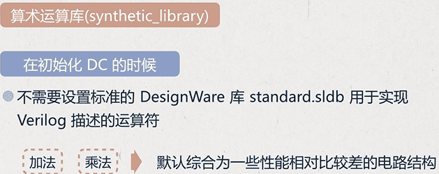
When DC is synthesized, the circuit structure is synthesized by default with relatively poor performance. For example, the adder (operator "+" in verilog) is synthesized into a serial carry adder. If you want to use a high-performance adder, such as a carry-lookahead adder, then you need to set up an arithmetic operation library and let DC call the Designware library during synthesis. At the same time, it is also necessary to set the corresponding library in 1ink_library so that DC can search for the implementation of the corresponding operator when connecting. (This is a more advanced function and requires an advanced license)
Article source
[1] https://www.icourse163.org/learn/SWJTU-1207492806?tid=1470116659#/learn/content?type=detail&id=1253638057&cid=1284287406
[2] https://blog.csdn.net/one11070910/article/details/128243158?spm=1001.2014.3001.5502
[3] https://blog.csdn.net/Tranquil_ovo/article/details/129876980?spm=1001.2101.3001.6650.3&utm_medium=distribute.pc_relevant.none-task-blog-2~default~CTRLIST~Rate-3-129876980-blog-111463698.235^v43^pc_blog_bottom_relevance_base2&depth_1-utm_source=distribute.pc_relevant.none-task-blog-2~default~CTRLIST~Rate-3-129876980-blog-111463698.235^v43^pc_blog_bottom_relevance_base2&utm_relevant_index=6