Clock tree synthesis is performed immediately after layout. Clock tree synthesis problem: Given the distribution of clock units, construct a clock network (tree) to achieve the timing requirements for the clock source to reach each register. During this period, the given various constraints must be met and design resources should be saved as much as possible. Let’s start with the generation of clock signals and understand the definition of clock signals, and then talk about clock tree synthesis.
1 Generation of clock signal
There are many ways to generate clocks. In VLSI design, a common method is to use an external crystal oscillator input (for details, you canclick here). For high-frequency clocks, dedicated phase-locked loop PLL circuits are often used for frequency multiplication.
In addition, clock generation methods include DLL, oscillation ring circuit, etc. (For detailed information, please refer to "Digital Integrated Circuit Physical Design P93-95").
2 Definition of clock signal
There are many characteristic parameters of a clock signal, but its three elements are the clock period (frequency), clock delay, and clock signal uncertainty. These three elements are usually defined in the SDC file using the create_clock and create_generated_clock design constraint commands.
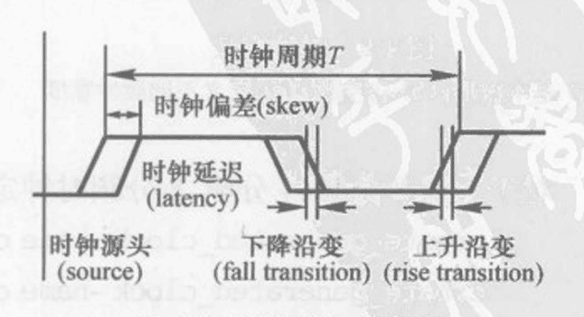
Clock Period: A clock period is the length of time that a complete cycle of a clock signal lasts. In digital systems, the operation of each logic element is driven by the rising or falling edge of the clock signal. A clock period defines the time it takes for a signal to change from one state to another within one cycle. The inverse of the clock period (that is, the reciprocal of the frequency) represents the frequency of the clock signal, usually expressed in Hertz (Hz).
Clock Latency: Clock delay is the time difference between a signal arriving at the clock input of a circuit element and the corresponding output of that element. Clock delays typically include time delays due to factors such as signal transmission, logic circuit delays, and timing dependencies. Clock delays are critical to ensuring the correctness and performance of a circuit because different signal paths may have different delays, potentially causing timing errors.
Clock Signal Uncertainty: Clock signal uncertainty refers to the inconsistency or fluctuation in the clock signal as it reaches different parts of the logic circuit. These uncertainties may arise due to different signal transmission paths, jitter caused by clock buffering, non-uniformity of the clock distribution network, etc. Clock signal uncertainty affects circuit stability and performance, so this uncertainty needs to be considered and minimized in the design.
(1) Definition of clock
- Basic clock definition
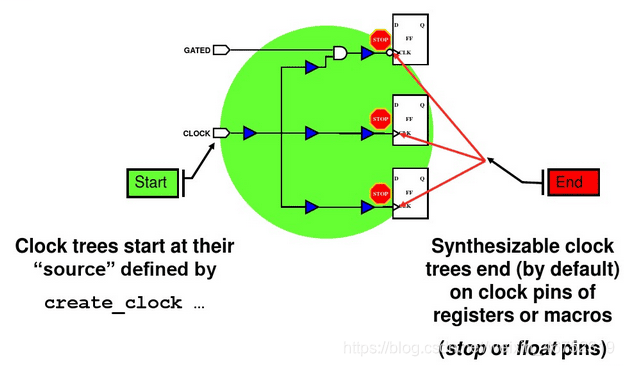
Generally, the clock starts from the clock source and ends at the CK end of the register. To define this kind of clock, use the command create_clock to define the root point of the clock. As shown in the figure below, CLKP is defined as:
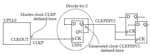
Icc_shell>create_clock -name CLKP [get_pins UPLL0/CLKOUT]
- Generate clock
The generated clock is obtained by multiplying the ordinary clock through the PLL, and the ordinary clock is called the master clock of the generated clock. The CLKP in the above figure is the main clock that generates the clock CLKPDIV2. Define the root point command for this generated clock:
Icc_shell>create_generated_clock -name CLKPDIV2 -source UPLL0/CLKOUT -add -master_clock CLKP -divide_by 2 [get_pins UFF0/Q]
What is the difference between source clock and master clock?
Source clock usually refers to the clock signal provided externally to the chip, also known as the clock signal of the input circuit. For example, some chips may require an externally input reference clock signal to synchronize all modules running inside them. In this case, the input reference clock is the source clock. When designing a circuit, you need to ensure that the source clock meets the timing requirements in the chip specification to ensure the correctness of the circuit function.
Master clock usually refers to the main clock signal inside the chip, also called the system clock or local clock. The main clock is a synchronous clock signal for each module inside the chip. It is used to ensure the timing and synchronization of various logic components inside the chip to provide reliable electrical performance. Usually, the chip will have a main clock generation circuit to generate a basic clock signal, and then generate different clock domains through frequency division, phase adjustment, etc. to meet the timing requirements of different logic units.
Therefore, source clock and master clock are both clock signals, but source clock usually refers to the clock signal input from outside the chip, while master clock is the main clock signal used and distributed inside the chip. They play different roles in circuit design and need to be correctly selected and used according to specific chip design requirements.
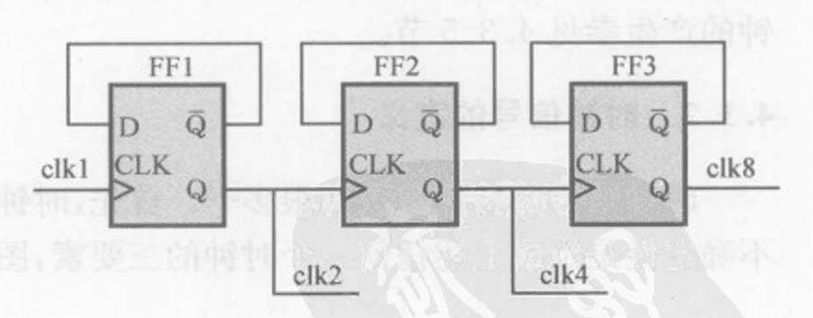
The definitions of the above divided-by-2, divided-by-4, and divided-by-8 clocks are as follows:
create generated clock -name clk2 -source clk1 -divide by 2 FF1/Q
create generated clock -name clk4 -source clkl -divide by 4 FF2/0
create generated clock -name clk8 -source clk1 -divide by 8 FF3/0
(2) Clock signal delay (latency)
Clock signal delay (latency) includes clock source (clock source) insertion delay (insertion delay) and clock network (clock network) insertion delay.
Clock source insertion delay: the delay between the system (that is, the clock source or from the chip) and the current chip (or to the current module) clock root node (clock root pin);
set_clock_latency 2.0 -source [get_clocks {cpu_clk}]
Clock network insertion delay: the delay of the clock tree;
set_clock_latency 2.0 [get_clocks {cpu_clk}]
Total insertion delay: the insertion delay from the clock source to the clock tree register;
Total insertion delay = clock source insertion delay + clock network insertion delay
The definitions of clock source insertion delay and clock network insertion delay are distinguished by the -source option.
(3) Clock signal jitter (jitter)
Clock jitter is defined as the deviation between signal time and ideal event time. Jitter contains deterministic jitter (DJ) and random jitter (RJ) components.
The jitter of the clock signal is also called the uncertainty of the clock. During the clock tree synthesis, the clock jitter cannot be optimized accordingly, and its impact can only be taken into account. It can be seen that the jitter exists innately, and the uncertainty is artificially defined. When establishing an ideal clock, we use the set clock uncertainty parameter to set the jitter value. For example:
set clock ucertainty 0.3 [get clock{*}]
This sentence defines that there is an uncertainty of 0.3ns on all clock signals. In general, during the logic design stage, the uncertainty of the clock is set larger to reserve a certain range for the comprehensive skew value of the clock tree. After the clock tree is synthesized, this value can be set smaller, generally depending on the process and design conditions. After clock tree synthesis, the real clock replaces the ideal clock. If the clock jitter is not considered, its value is set to zero. If the clock jitter is considered, the jitter value is set to the real jitter value of the clock under the corresponding process conditions.
(4) Clock signal deviation (skew)
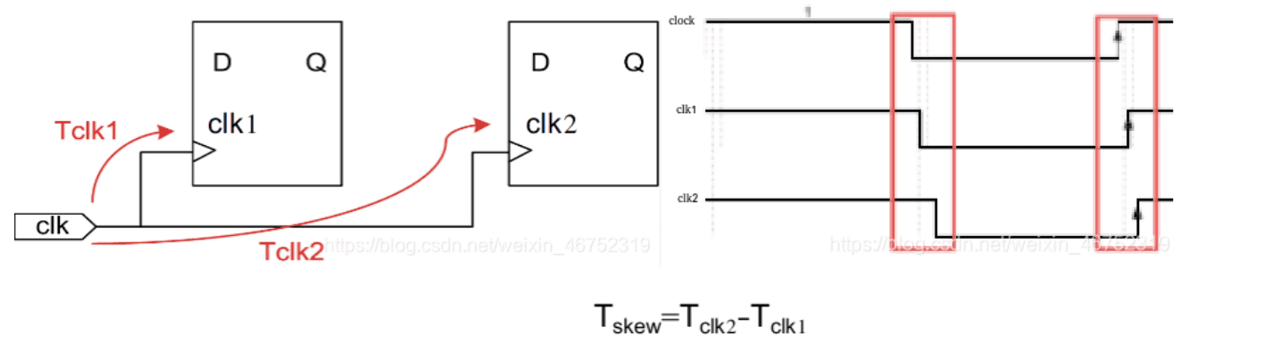
The deviation of the clock signal refers to the time deviation between the same clock arriving at different registers in the clock domain, that is, $$skew = max (|t_i-t_j|), 0<i,j<n$$
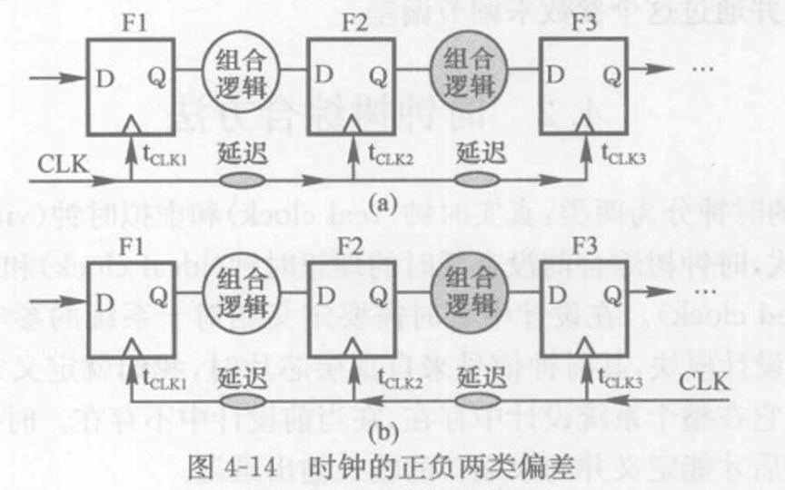
ti,tj are the time when the clock root node reaches the leaf node respectively, and n is the number of sequential units in the same clock domain. The purpose of clock tree synthesis is to reduce deviation, and its value has both positive and negative values.
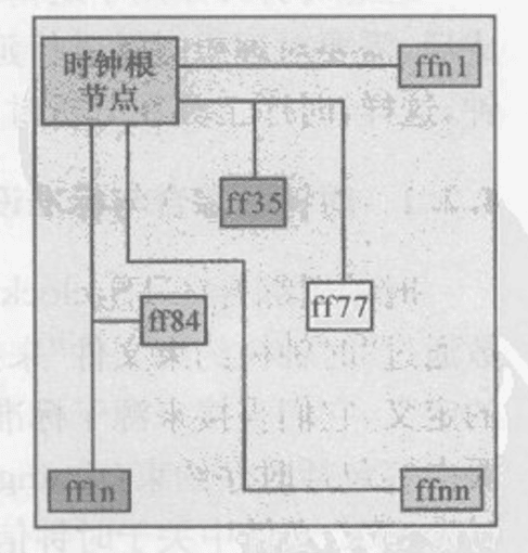
An example of the deviation is shown in the figure below. Due to the different lengths of the clock traces, the time from the root node of the clock to several leaf nodes is different. Assume that the time to arrive at ff35 is the earliest and the time to arrive at ffnn is the latest. The time difference between any two is called a deviation. In the application of clock tree, the latest time to arrive at ffnn is also defined as the "maxinsertion delay", the earliest time to arrive at ff35 is defined as the "mininsertion delay", and the difference between the two is defined as the "max skew". In large-scale integrated circuit design, the large-area distribution of tens of thousands of leaf nodes will cause the value of this deviation to be very large, resulting in a loss of chip performance. An important indicator of traditional clock tree synthesis is to achieve theoretical "zero skew".
The time for the clock to reach leaf nodes such as flip-flops ff1n, ff2n,…,ffnn from the root node is the clock delay. It can be seen that the clock delay exists within the maximum (insertion) delay and minimum (insertion) delay range (Figure 4-16). The actual deviation generally obeys the normal distribution (Figure 4-17). When establishing an ideal clock, a maximum deviation value needs to be proposed. After clock tree synthesis, the clock is set as the propagated clock during timing analysis, so that the actual clock replaces the ideal clock.
The delay definition of the ideal clock is used to control the number of driver units inserted in the clock tree. Generally, when the delay is large, the clock deviation will be smaller, but more buffers will be inserted, and the power consumption in the clock tree will be larger. When the delay value is small, the clock deviation requirements may not be met, so during clock tree synthesis, it is necessary to weigh the power consumption and clock deviation requirements to select an appropriate delay. Sometimes for some specific designs, a certain phase difference is required between the two clock domains, and the deviation can be adjusted through this parameter.
2 Introduction to clock tree synthesis issues
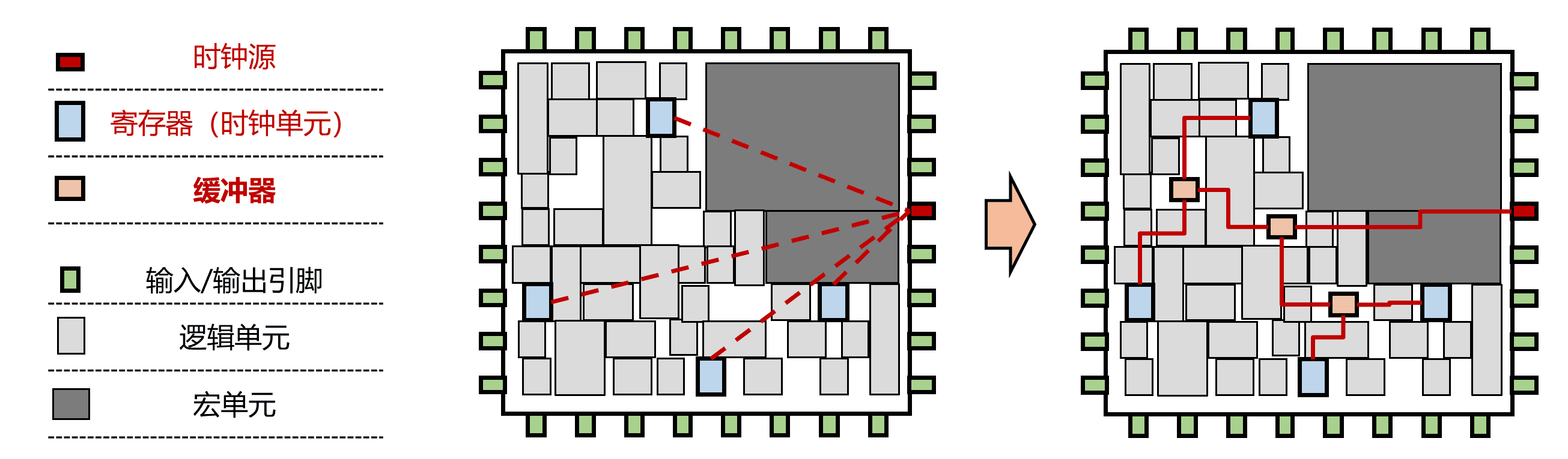
The process of clock tree synthesis is to build a clock tree from clock source to register so that the timing of each path meets the design needs. The tool attempts to make all sinks belonging to a certain clock the same length, that is, to make the time it takes for a clock signal to reach each terminal node to be the same as possible. As shown in the figure, the clock tree solution mainly consists of inserting buffers and building a line network topology.
Before clock tree synthesis is performed, the clock tree has not yet been generated. The clock logic structure is as shown in the figure on the left. A clock source terminal (root) eventually fans out to the clock terminals of many registers. But we know that the drive and load of the path that the clock source takes to reach different registers are different, so the time when the clock signal reaches the clock end of each register is also different. The time deviation when it reaches different registers is called skew. Traditional CTS is to reduce skew.
After clock tree synthesis, a clock tree is formed by adding small orange squares (buffers) as shown in the picture on the right. The clock signal will first reach the buffers at all levels so that the time it finally reaches the clock end of each register is almost the same.
Therefore, the purpose of clock tree synthesis is twofold:
The clock skew should be as small as possible, especially for clock quality requirements or high-frequency clocks;
Clock latency should be as short as possible.
Clock tree synthesis implementation
(1) Insert buffer buffer
In the clock line network, buffers can play the role of decomposing the line network. For example, by inserting two buffers in the figure, the original 4 fan-out structure can be converted into three 2-fan-out structures.
The buffer can also enhance the driving capability, because the conversion of high and low levels during signal propagation takes time, and the buffer can effectively reduce the conversion time and enhance the driving capability.
If a buffer with strong driving capability is used, the signal conversion can be completed in a shorter time. Inserting a buffer on a longer wire can effectively reduce the delay. Continuously inserting multiple buffers can increase the path delay. Therefore, the impact of inserting a buffer on the timing is very significant.
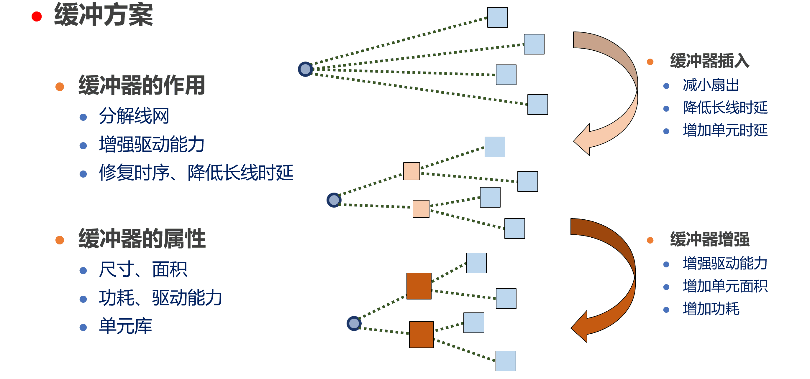
Different buffers will have different properties:
We will pay attention to the size and area of the buffer, because this will affect the layout resource utilization
At the same time, we are concerned about its power consumption and driving capability. Generally speaking, the stronger the driving capability, the larger the area, and the power consumption will be higher for the design.
These attributes are in the unit library corresponding to the buffer, and its delay for different line network conditions is also obtained through the unit library table lookup.
(2) Construct line network topology
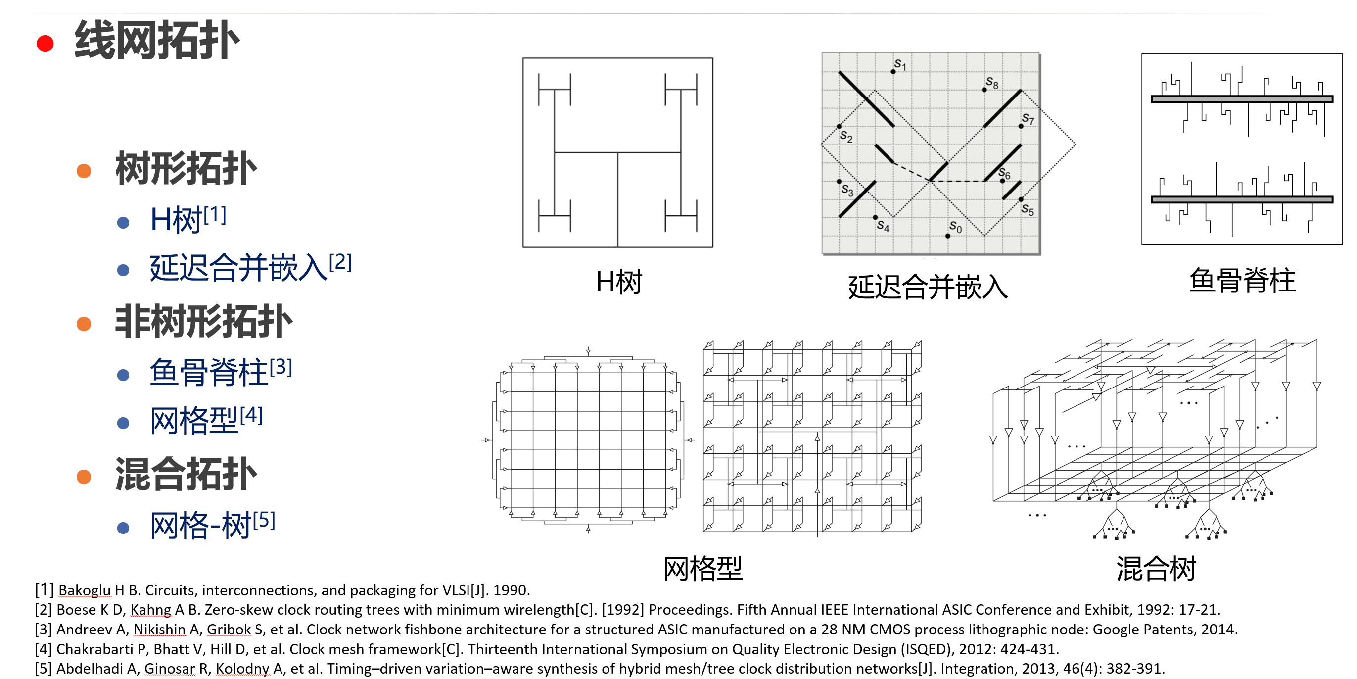
The early clock tree designs were small in scale, and in some cases there was no need to consider the use of buffers to balance timing and solve driving capability issues. Therefore, the research on clock tree network topology is relatively sufficient, and many types of construction methods have been developed, which can be roughly divided into three categories:
- The first type is tree topology
More typicallyH-tree,Using the fractal characteristics, a completely symmetrical ,balanced tree structure can be built, so the clock deviation is ,small, but the bus length of this kind of tree has a large ,delay.
Another category isDelayed merge embedding algorithm, it merges two subtrees or nodes each time, and each merge calculates the feasible solution area of the parent node until the clock source, thereby ensuring that the clock deviation is always within the allowed range. Mainly used are greedy or merging methods of a given graph structure.
- The second type is non-tree topology
The fishbone spine topology uses metal trunks and branches to directly drive load units. This method has shorter line length and lower latency. However, clock deviation can only be effectively controlled when the load units are distributed more concentratedly.
The grid topology uses a two-dimensional grid structure and has good robustness and scalability, but its design cost is high and it is difficult to perform verification and timing analysis.
The third category is hybrid topology
This type of topology combines grids and trees for hierarchical design, which can weigh their advantages and disadvantages.
Click here for detailsvideo。
Original link:https://blog.csdn.net/weixin_46752319/article/details/107387584