The logic synthesis phase outputs the gate-level netlist and design constraint file (SDC), and then enters the physical design phase. The physical layout of a chip design is often referred to as place and route (PnR), which is not that accurate. A lot of work before layout including floorplan and powerplan is often ignored.
If we make an incomplete analogy between chip manufacturing and building a house, layout planning is equivalent to the preliminary design drawings of the house, which roughly determines the shape, size and layout of the building; power planning, as its name suggests, plans the overall power cord layout of the building; layout formally determines the functional areas of each house type, and the locations of floor drains, power sockets, etc. in each room to facilitate subsequent ducting (wiring).It should be noted that the three tasks of layout planning, power supply planning and layout are usually carried out continuously, but they are often interspersed and repeated in the project.
1 layout planning
Layout planning and layout occupy an important position in chip design. Whether it is reasonable or not is directly related to the timing convergence, smooth wiring, power supply stability and yield rate of the chip. Therefore, in the entire chip design, layout planning to completion of layout generally takes up 1/3 of the entire physical design time. Simply put, the key to layout planning and layout isHow to reasonably divide areas and place units to make various performances as optimal as possible. Below we will introduce the input files, Main topics and goals of layout planning.
(1) Input file for layout planning
The layout planning input file is as follows:
| Type | Kind | Features |
|---|---|---|
| Design netlist | gate-level netlist (e.g., chip_design.v) | single complete file |
| design constraint file | chip_design.sdc | single complete file |
| physical library file | standard.lef, io.lef, rom.lef, ram.lef | Documents related to timing requirements |
| Timing library file | standard.lib, io.lib, rom.lib, ram.lib | Single complete file or multiple files |
| I/O files | I/O constraints file | Single complete file or multiple files |
| Layout requirements document | floorplan configuration file | single file |
Netlist files and SDC files are generated during the logic synthesis stage, while LEF files, LIB files and I/O files are provided by the foundation.
(2) Main topics of layout planning
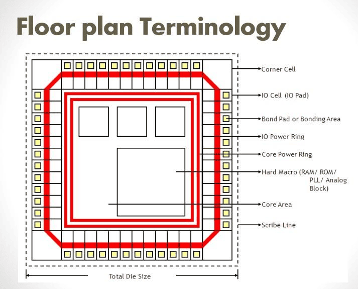
Chip size (die size) planning
Chip design input/output (I/O) unit planning
Planning of a large number of hard cores or modules (hardcore, block)
......
In some irregular designs, some special settings are required for the wiring channels, and the setting of these parameters is also an integral part of the layout planning. In some more complex VLSI circuit designs, in order to minimize the deviation of clock signal lines and improve chip performance, the clock network needs to be planned before layout. The clock network distribution at this time is different from the ordinary clock tree, and it is also an important part of layout planning. It can be seen that the content of layout planning is the complete planning and design of the internal structure of the chip.
[Note] What is the difference between hardcore, block and macro?
In the world of chip design, the terms "hardcore", "block" and "macro" are often used to describe different levels of IP or modules. The differences between them are as follows:
Hardcore:
- Hardcore IP refers to the IP core that is pre-designed and implemented in chip design and is usually provided by the chip manufacturer.
- These IP cores are typically optimized for specific hardware architectures and processes, with fixed functionality and performance characteristics.
- Hardcore IP is often highly customized, highly integrated, and difficult to modify or customize.
Block:
- Block usually refers to a functionally relatively independent block or module, which can be a unit in hardware design.
- These blocks can be general and reusable, or customized and targeted to specific functions.
- Blocks can be combined and reused in designs and are often used to build complex systems.
Macro:
- Macro usually refers to a larger functional unit than block and can contain multiple blocks or other logical units.
- Macros can be reusable functional modules with interfaces, or customized functional units for specific application scenarios.
- Macros provide a way to encapsulate complex functionality into a single unit for ease of use.
In general, hardcore is a pre-designed IP core, block is a relatively independent functional module, and macro is a larger functional unit that can contain multiple blocks. These terms help engineers perform modular design and combination in chip design to improve design efficiency and reusability.
(3) The difference between layout planning and layout
Floor planning and layout both involve placement, but they place different things:
Layout planning determines the module size, location, shape, and placement of Macro, which is the random memory unit RAM, read-only memory unit ROM, and other IP modules we usually see.
The layout mainly places standard units, and the standard units have a certain height and the width is an integer multiple of the site. (If you are not familiar with it, please read the LEF file introduction)
Difficulties in layout planning compared with layout: The shape and size of the module may be an uncertain variable, and the results need to be weighed to infer this variable.
The difficulty of layout compared with layout planning: the overall data volume is not very large. In other words, there are too many standard units.
(4) Objectives of layout planning
The layout planning is done, so how to determine whether it is "ok"? This involves the goal of layout planning. The four goals are as follows:
Determine the area of the chip. For cost reasons, the smaller the chip area, the greater the number of die produced on each silicon wafer (wafer), thereby reducing the average cost per chip. However, if the die area set in the layout plan is too small, it will cause high congestion and difficulty in wiring, which will lead to long-cycle design iterations. A reasonable area setting is to save product costs as much as possible while ensuring wiring, so the initial goal of layout is to estimate the size of the chip area.
Ensure timing closure. In digital integrated circuit design, all work is completed under the control of clock beats, so the length of the path from one register to another register determines the performance of the chip. In the layout planning stage of chip design, designers must consider whether the final chip can meet the design's standard timing constraints (SDC) requirements, achieve timing convergence, and meet the performance that the chip needs to achieve. Therefore, the chip delay needs to be estimated during the layout planning stage.
Ensure the stability of the chip. The stable operation of the chip is an important part of the chip's value. The electrostatic protection of the chip's input and output units and the power supply design of the input and output units are important conditions for ensuring the stability of the chip's input and output. Power supply planning is also a necessary condition to ensure uniform power distribution within the chip, sufficient power supply, and stable chip operation.
Meet the wiring requirements. Layout planning and layout complete the device placement of the chip, and the realization of the chip function requires that all devices be wired as required. Therefore, the purpose of layout planning is to facilitate wiring. While ensuring smooth wiring, the length of the wiring should be shortened as much as possible, that is, the delay of the interconnection lines should be reduced, thereby effectively improving the performance of the chip. This requires the designer to have a certain understanding of the logic design and its functions, such as the connection relationship between each module, the data path structure, etc. There is a huge difference in timing between a good layout plan and a poor layout plan.
# If you want to expand your learning on "placement and power supply of I/O interface units, layout planning and delay estimation, module placement and wiring channels", please see "Digital Integrated Circuit Physical Design" P58-67.
2 Power planning
In chip design, power supply design is required after layout planning. For smaller chips, the process is to set up some simple power network cables, so power supply design is often considered to be part of the layout planning. As the size of the chip increases, power supply design becomes more complex. It is no longer limited to "grid" design. It is proposed to call it "power (ground) planning" to better reflect the actual situation of contemporary design. Therefore, in the process of physical implementation, from data input to clock tree synthesis, the content can be divided into three major items, namelyFloor planning, power planning and layout。
(1)Power planning goals
- Generate a power supply network that can meet IR drop (voltage drop) and EM (electromigration)
Chip power supply is realized through the I/O unit. When doing power supply planning and power network design, power budgeting must be done first. It is common practice for commercial products to believe that the total error should be controlled within ±5%. It includes the fluctuation from the power network and PCB board level to the package bonding (approximately ±1%), to the fluctuation between the power I/O unit and the power ring (approximately ±1%), and finally up to the voltage drop between standard cells (approximately ±3%).
Minimize routing track resources
Make DRC clean
(2) Introduction to power network
Global power connection relationships
That is, alobalnet connect, which refers to connecting the corresponding ports and networks to the appropriate power and ground networks. Part of the connection information of these terminals and networks is included in the Verilog netlist, and the other part is included in the corresponding LEF file. In the tool, it is actually the entire globalNetConnec command.
globalNetConnect VDD -type pgpin -pin vdd! -all
The above two commands indicate that the vdd! and gnd! pins of all instances need to be connected to the global VDD and GND network lines.
power ring
Refers to the power ring surrounding the entire core in order to provide uniform power supply. As shown in the figure below, the outer circle of the power core is the power ring.
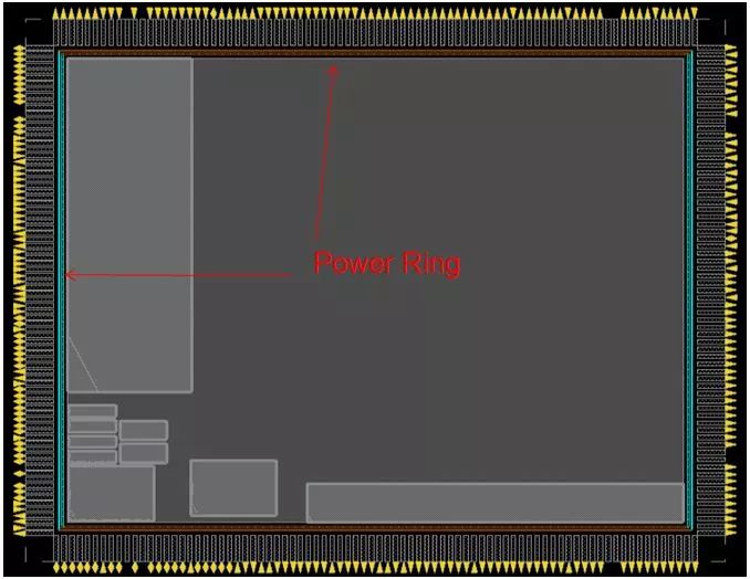
Hard core power ring
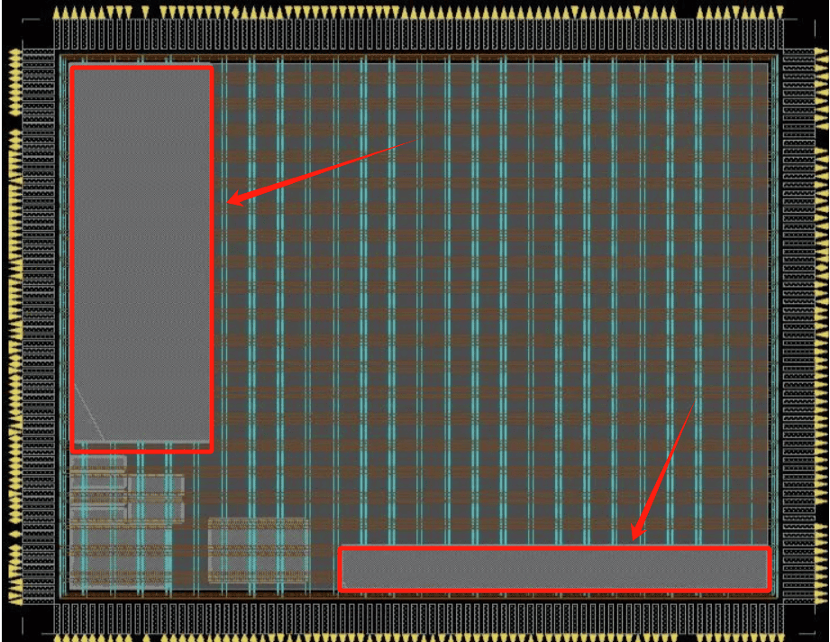
Hard-core power ring design, as shown in the figure:
I/O unit power ring
The design of the power loop of the I/O power supply unit is as shown in the figure:
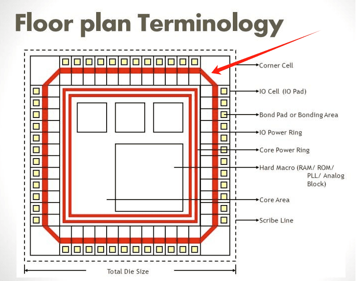
Among them, the connection between the power supply unit and the power ring is called the I/O unit power
power stripe
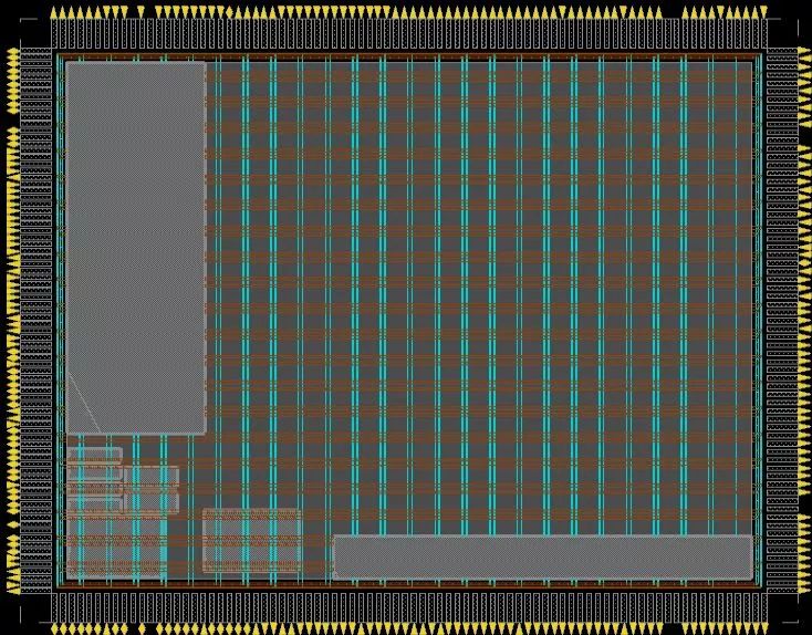
The criss-crossed power lines inside the chip are called power strip lines. Their purpose is to deliver power to each macro inside the chip, as shown in the figure below:
followpin(power rail)
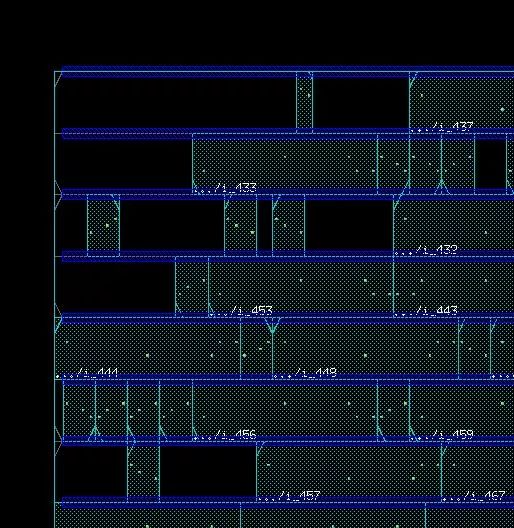
The power supply network of the standard unit is shown in the blue line in the figure below:
ring pins:
The pin connecting the power stripe inside the chip to the hard core power ring
Quote
[1] "Physical Design of Digital Integrated Circuits" P67-78
[2] https://blog.csdn.net/Tao_ZT/article/details/102456851
[3] https://mp.weixin.qq.com/s?__biz=MzU5NzQ1NDI5Nw==&mid=2247483900&idx=1&sn=f8807031da4d2aefd403ca8be449b38a&chksm=fe527d4ac925f45c4c7fbac3643bd6e98f00391762389f62e53014291e929cc6a1840d26171f&scene=21#wechat_redirect