The placement of I/O units and modules in the layout category is completed during layout planning, and the layout plan is determined——Flat layout or hierarchical layout, so the remaining tasks of the layout are mainly to lay out the standard units according to the layout plan.For the specific types and functions of standard units, please move to Part 4.。
1 Contents of the layout
Placement detailed steps
(1)Initial placement
This step is what we usually call the initial layout, also called Coarse placement. In this step, the EDA tool will initially place the components in the circuit (such as logic gates, memory, etc.) on the physical space of the chip based on the design specifications and layout constraints. This placement is based on the initial algorithm and is usually not optimal. The overlap issue is not considered at this time. The Overlap problem refers to a common challenge in circuit layout, that is, different circuit elements (such as logic gates, memories, etc.) overlap or conflict with each other in physical space.
(2)Legalization
After the coarse placement in the first step, this step requires legalization of the roughly placed cells, placing all standard cells on the rows, and ensuring that all cells are in a legal state, that is, there is no overlap or they are not on the corresponding row. Legality refers to adjusting the position, spacing, alignment, etc. of unit components to ensure that the layout meets the circuit design requirements and does not cause conflicts.
(3)Removing existing buffer trees
This step is called Removing existing buffer trees. In some circuits, buffers may be added to account for timing issues and signal delays. However, during the layout process, it may be decided to remove part of the buffer in order to reduce power consumption and signal line length. This step involves removing part of the buffer tree from the layout and rearranging the related components.
(4)High Fan-out Net Synthesis (HFNS)
In circuit layout, High Fan-out Net Synthesis (HFNS) is an important step. It is mainly optimized for points with high fanout (except for special cases such as clock signals and reset signals) to improve the timing performance of the circuit. Before proceeding with HFNS, there are some design constraints that need to be considered, and unnecessary ideal nets should be removed as much as possible to improve layout quality.
(5)Iterations of timing/power optimizations
This step is called Iterations of Timing/Power Optimizations (timing/power optimization iterations). At this stage, iterative optimization techniques are used to improve the timing and power consumption of the circuit. This includes optimizing critical path delays, optimizing the re-layout of logic components to reduce power consumption, adjusting component location and routing, etc. The goal of iterative optimization is to meet the design's timing constraints and reduce power consumption. This process mainly consists of small steps such as cell sizing, moving, net spitting, gate cloning, buffer insertion and area recovery.
(6)Scan-chain re-ordering
Scan chain reordering (scan chain reordering) is not done in every design, depending on the situation. This process is mainly used to alleviate the problem of tight winding resources. Scan chains are an important component for testing and troubleshooting circuits. This step involves reordering scan chains to optimize test time and fault coverage. Reordering can be accomplished by adjusting the order of elements in the scan chain.
2 Objective evaluation of layout
After the layout is completed, how to evaluate the quality of the layout? inMeet design rule requirementsIn this case (that is, in addition to the clock network, other high fan-out networks, such as reset signals, etc., are inserted into the corresponding driving units to meet design constraints such as maximum capacitance, maximum fan-out, and maximum signal conversion time. The design rules on the clock network need to be completed in the clock tree synthesis stage), which can be summarized into the following three parts:
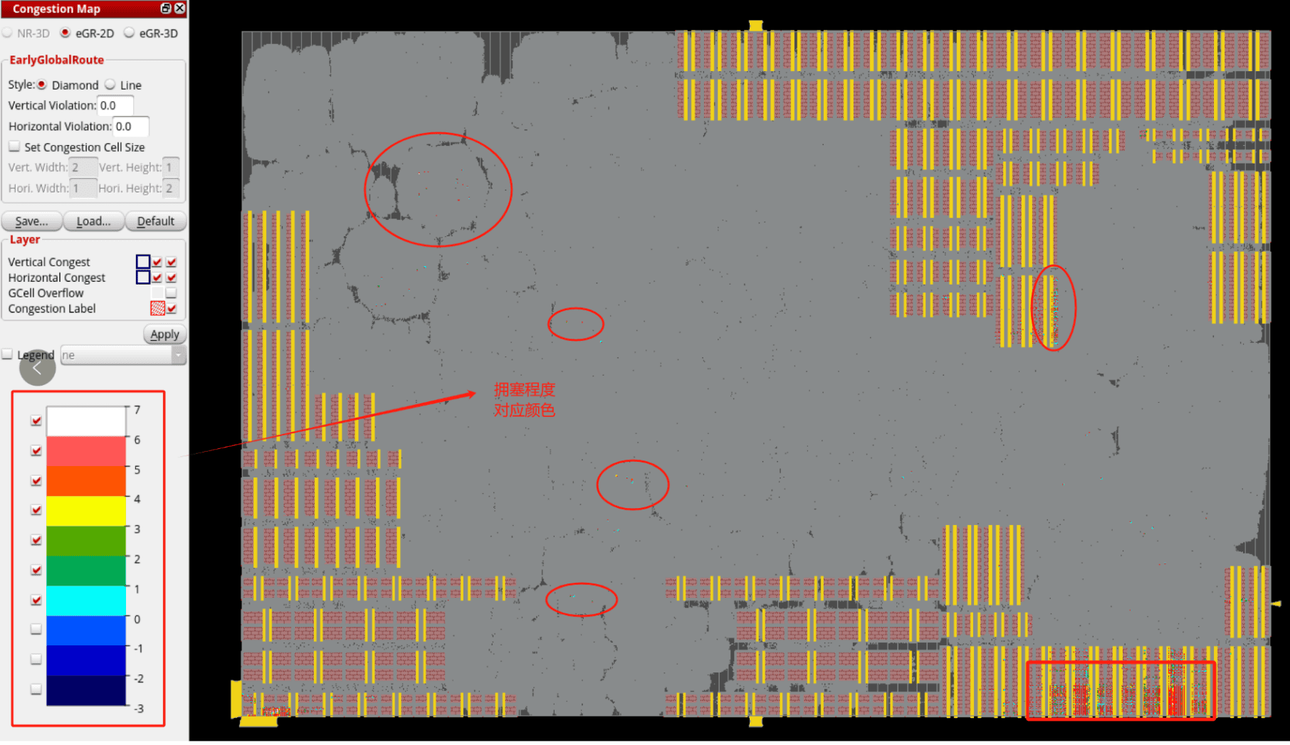
congestion estimate
The requirements are to meet the requirements of wiring routing. The EDA tool divides the entire wiring space into multiple small wiring grids, and each wiring grid is divided into horizontal channels and vertical channels. Within each wiring grid, the number of vertical channels and horizontal channels required is estimated and counted. When the actual required channels exceed 5% of the existing channels, it indicates that the degree of congestion is relatively large. Using the EDA tool to analyze congestion and display the congestion level menu, the congestion data and distribution can be obtained to determine the layout optimization plan. When global congestion is small but local congestion is large, the design needs to be optimized. When the global congestion is reported to be very small, but there is large congestion in local areas, which will cause the wiring to be unable to be routed, the standard cell layout needs to be optimized.
Timing estimation
Setup time requirements are required. After the standard unit layout is completed, its positions are relatively determined. At this time, the delay calculation and timing of the chip are closer to the final timing of the chip. After the layout is completed, generally you only need to doSetup time estimate, there is no need to estimate the hold time because clock tree synthesis has not yet been performed, and hold time violations are usually optimized after clock tree synthesis.
At this time, the impact of noise can also be estimated. In processes of 0.18um and above, noise generally does not need to be considered too much, while in processes of 0.13um and below, the impact of noise needs to be considered, and noise can be considered in the standard cell layout stage.
Power supply estimate
It is required that the standard unit can supply power smoothly. After the standard unit is laid out, connect the power supply port of the standard unit to the power grid (followpins). At this time, you can quote the VCD file to evaluate the chip's power consumption, voltage drop and EM. Since the clock tree has not yet been synthesized, the power consumption value will be too small, so care should be taken when estimating.