Placement and clock tree synthesis are followed by routing operations. Main topics: To complete the connection of signal lines of standard units, wiring tools need to consider issues such as eliminating wiring congestion, optimizing timing, reducing coupling effects, eliminating interference, reducing power consumption, and ensuring signal integrity.Due to the large scale of circuits (millions, tens of millions), complex wiring problems, and high time complexity of direct solution, wiring is divided into global wiring and detailed wiring.
1. Gcell Grid
Gcell Grid is a grid structure used for grid management in chip layout. It divides the chip surface into a series of regular square or orthogonal grid units, each unit is called a Gcell. The purpose of Gcell Grid is to simplify the layout, wiring and implementation process and ensure that the timing and wiring rules of the design are met.
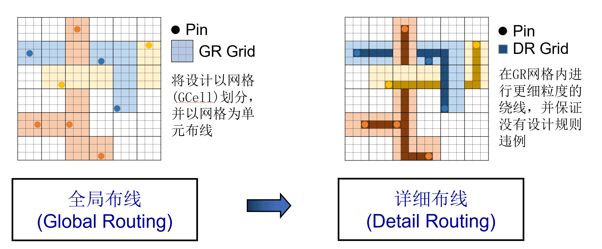
Now let's talk in layman's terms why we should build a Gcell Grid. If the wiring project is compared to a 1,000-piece puzzle project, it is obvious that we need to divide the large puzzle into blocks with different characteristics (Gcell Grid), and then divide the scattered puzzle pieces into blocks and divide them into several piles (global wiring), and then splice each pile (detailed wiring). Another use of Gcell Grid is to evaluate the degree of congestion. See the 2 Global Routing section for details.
Based on the grid wiring theory, the length and width of the grid are defined in the Lef or floorplan file (.def). Of course, the tool will automatically generate it initially based on the design and technical lef conditions. As shown in the figure, during global wiring, each black box is a Gcell. Those with the same color need to be routed. The specific wiring will occur during detailed wiring.
2 Global Routing
Global routing Global routing, referred to as GR. It does layout planning for the wiring of the entire chip and does not perform any actual wiring (not lay down any metal traces)
GR will allocate lines to the specified metal layer and Gcells, and judge the congestion level based on the number of allocated lines.
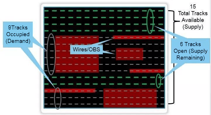
The above picture is an example of a GCell. As shown in the picture, a GCell contains 15 tracks (usually a gcell will occupy more than 10 tracks, which vary depending on the design). Among them, 9 are occupied due to wires or OBS (route blockage), etc. and the remaining 6 are available for use. The goal of global routing is to keep the capacity occupancy of each gcell at about 85%.
In this figure, demand = 9, supply = 15, then congestion = demand - supply = -6 (negative values indicate no congestion, and the greater the positive value, the higher the degree of congestion)
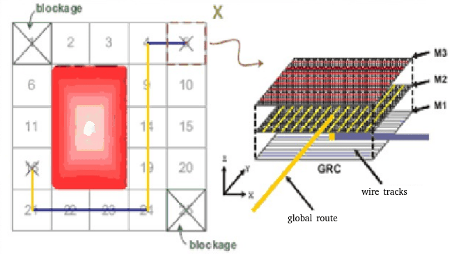
The numbers on the grid indicate the degree of congestion. The global route uses gcell cells as the routing reference grid. When routing, the tool will try to avoid gcells with high congestion and find the shortest path in the gcell. In the global route, the software only knows the starting point and the end point, which can be simply understood as two pins with a connection relationship. But I don’t know how to get from the starting point to the end. However, GR will avoid areas with high congestion, blocks, and P/G (rings/straps/rails), so that a rough routing path can be roughly designed.
3 Track Assignment
GR is based on the analysis of gcell. It mainly allocates routing resources. According to the global routing results, you can check the congestion situation, which is to check whether the routing resources are sufficient and reasonable. It does not allocate routing to specific tracks. Track Assignment (TA) assigns each connection in the GR design to a certain track, and performs actual wiring on the connection. No DRC check is performed at this stage.
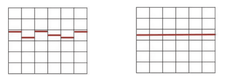
As shown in the picture above, the left picture is the net formed by GR, and there is no end-to-end connection. After track assignment, the complete net in the right picture is formed. Moreover, during the track assignment stage, the wiring should be as long and straight as possible, but this will also reduce the number of holes. In order to reduce the number of holes, jog will be formed (changing the wiring direction in a small range, as shown in the figure below).
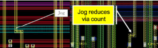
The TA phase does not check DRC, that is, routing will generate many DRCs: Wire spacing; Wire width; Via rules (size; density; stackable etc..), which is fixed by Detail Route.
4 Detail Route
The work of Detail route is mainly to remove the DRC violation generated by TA. Method: Use a fixed size switch box (sbox) to fix the violation. Sbox is a small grid evenly divided into the entire layout. The tool repairs the DRC inside each small grid, but the DRC on the border cannot be repaired.
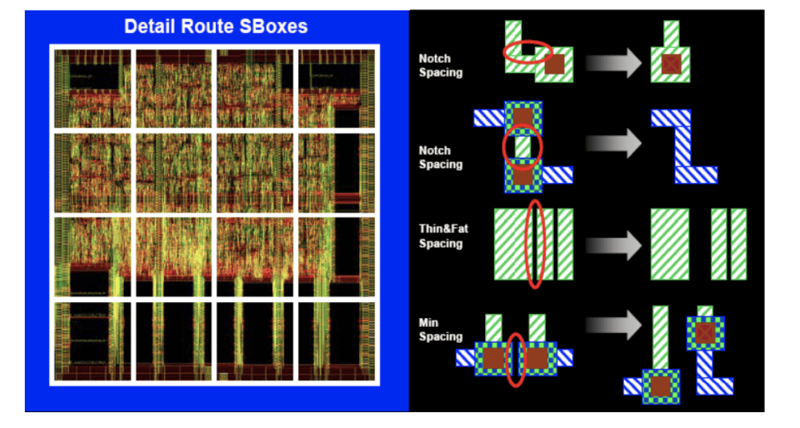
Sbox is composed of GCell, and the edge of each Sbox will overlap by one GCell width (Sbox is composed of GCell, and the overlap width of two sboxes is the width of one GCell).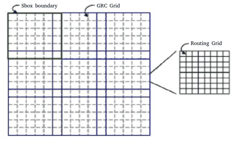
5 Search and repair
Search and repair (wiring repair), by gradually increasing the size of the Sbox to find and eliminate DRC violations that have not been completely eliminated in Detail routing.
Quote
[1] https://vlsi.pro/physical-design-flow-iv-routing/
[2] https://blog.csdn.net/Tao_ZT/article/details/102456868
[3] https://blog.csdn.net/sinat_41774721/article/details/123430167
[4] "Physical Design of Digital Integrated Circuits" P128-138