Well tap cells (or tap cells) are used to prevent latch-up in CMOS designs. Covered in Part 4: Latch-up Effects. The well plug unit connects nwell to VDD and p-substrate to VSS to prevent latch-up issues. The well plug unit has no logical function and only provides a connection between nwell and p-substrate, so the well plug unit is called a physical unit only. In this article, we will discuss the structure of well plug units, the requirements for well plug units, and how to place them in the physical design process.
1 Well plug unit:
The well plug unit has no logical function and only has two connections.
- nwell to power supply (VDD)
- p-substrate to ground (VSS)
The typical structure of well bolt layout is shown in Figure 1. The well plug unit has no input and output pins, so it is called a physical unit.

Figure 1 Layout of well plug unit
2 Why the well plug unit is needed:
latch up (door lock effect), in the CMOS process, due to the existence of npn and pnp transistors, as well as the existence of parasitic resistances Rw and Rs, the two transistors are coupled to each other to form an SCR. Once a certain transistor has sufficient base bias voltage, the SCR enters the working state and the current is continuously amplified, which will cause a huge conduction current to form between the power supply and the ground and burn out the chip.
One function of the Tap Cell is to apply a bias voltage to the substrate at a fixed distance to reduce the parasitic resistance of the substrate, so that the transistor cannot meet the conduction requirements, thereby cutting off the positive feedback loop of the latch effect and eliminating the latch effect.
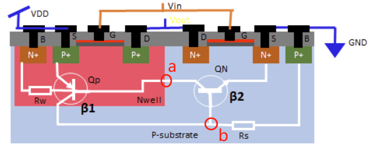
Figure 2 The role of tap cell in the latch effect
Why does the source of the MOS tube have two active areas (the source of NMOS has an extra P+, and the source of PMOS has an extra N+)? It should be to clamp the substrate voltage to 0 or to 1 to prevent latch-up effects. Even if the high voltage at point a in Figure 2 does not cause the PNP transistor to turn on, maintaining the low voltage at point b will not cause the NPN transistor to turn on.
Why are the two active regions (heavily doped regions) of the source region of the MOS tube different types, for example, the active region on the left side of the source of the NMOS is P+, not N+? It itself prevents latch-up. If N+ is used, an additional parasitic bipolar transistor structure will be formed, which will not be effective, but will be a disservice.
However, if a clamp electrode is made for each mos tube, the area of the standard cell will increase significantly, which is not conducive to the design of PPA; then an idea called "batch mode" (Chinese meaning "batch processing") comes into play. Instead of making a clamp electrode for each standard cell, can we make the clamp electrode into a standard cell separately, and then let the standard cells at a certain distance (commonly used is 50um) share a clamp electrode? This is the so-called batch mode idea. Then well tap came into being at this time.
In the early days, there was no concept of well plug cells. In the standard cell design, each standard cell had internal connections from nwell to VDD and p-substrate to VSS. But this standard cell design took up more area, and in order to save space, the concept of wellless battery cells later evolved. In a wellless battery unit, there is no well laying inside the standard cell, the well laying is provided by a separate standard unit called a well plug unit. Therefore, the well plug element is part of the wellless standard element library. Figure 3 shows the structure of a traditional standard unit and a wellless standard unit.
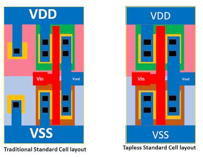
Figure 3 Structure of traditional standard unit and wellless standard unit
Well tap is used to prevent latch-up problems in CMOS designs. Well tap connect nwell to VDD and p well to VSS to prevent latch-up issues. There is no logical function in the well tap cell, so the well tap is also a physical only cell.
3. Placement of well plug unit:
Well plug cells are placed after macro cell layout and power track creation. This stage is calledpre-placement phase. Well plug units are placed at intervals within each row. The maximum distance between well plug units must comply with the DRC rules of the specific technology library. Figure 4 shows typical placement of well plug units. As a standard unit, the length of the well plug unit is an integer multiple of the site.
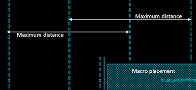
Figure 4 Placement of well bolt unit
Well plug units are typically placed in straight columns in alternating rows, forming a checkerboard pattern to provide maximum coverage of the well plugs. If a macro is located on the path of a vertical column, the placement of the vertical column will move with the macro, as shown.
The placement is performed using PnR tool commands. For ICC and Innovus tools, use the following commands to place well plug elements.
For Innovus tools:
set_well_tap_mode -rule <> -bottom_tap_cell <cellName> -top_cell_name <cellName> -cell <> addWellTap -cell <cellName> -cellInterval <maxGap> -prefix <prefixName> -checkerBoard -fixedGap verifyWellTap -report <reportName>
For more details, please refer to the Innovus tool's user guide.
For ICC tools:
add_tap_cell_array –ignore_soft_blockage true –master_cell_name $tapCell–distance $tapPitch –connect_power_name VDD –connect_ground_name VSS –respect_keepout-pattern stagger_every_other_row –tap_cell_identifier WELLTAP
link
[1] https://teamvlsi.com/2020/08/well-tap-cell-in-asic-design.html