In today's era of rapid technological development, the demand for low-power application scenarios is increasing, especially for handheld electronic devices. Among many handheld products, users hope to have longer battery life. We can only achieve this goal by ensuring that the system-on-a-chip (SoC) embedded in the device consumes less power. Currently, a variety of techniques are used in low-power designs to reduce the power consumption of application-specific integrated circuits (ASICs). Among them, integrated clock gating (ICG) technology is one of the important technologies widely used in low-power design. This article will introduce the architecture, function and layout of the ICG circuit in detail.
Why use ICG circuit?
The reason for using ICG circuits is that up to 40% or more of the chip's power consumption is consumed by the clock tree. The clock tree has the highest switching frequency in the system and contains many clock buffers with high drive strength to minimize clock delays. At the same time, even if the input and output remain unchanged, the flip-flop receiving the clock will consume a certain amount of power, especially dynamic power. In order to reduce the power consumption of the clock network, the most direct way is to turn off the clock when it is not needed, that is, to use clock gating: clock gating. By introducing a low-level clock enable signal into the ICG circuit, the transmission of the clock signal in the circuit can be effectively reduced, which is called clock gating. When a large logic unit does not need to be operated, the ICG circuit can be used to prevent the clock signal from propagating to the unit. The use of ICG circuits helps reduce dynamic power consumption because the clock tree contributes significantly to dynamic power consumption, and the ICG circuit allows the propagation of the clock signal to be stopped after it. Therefore, using ICG circuits is an effective way to reduce chip power consumption, improve chip performance and extend the battery life of the device.
Architecture of ICG circuit:
The ICG circuit is a circuit used to control clock signal transmission, which can effectively reduce chip power consumption. A common ICG circuit design is based on a latch and AND gate structure.
In this design, a latch is used to store the clock signal and is connected to an AND gate. The other input of the AND gate is connected to an enable signal (EN) source. When the enable signal is high, the output of the AND gate is controlled by the clock signal, which propagates to the rest of the circuit. When the enable signal is low, the output of the AND gate will be turned off and the clock signal cannot propagate.
The working principle of this ICG circuit based on a latch and an AND gate is as follows: when the enable signal is high, the output of the AND gate is connected to the input of the latch, and the clock signal can pass through the latch and propagate to the next stage of the circuit. When the enable signal is low level, the output of the AND gate is low level, and even if the clock signal exists, it cannot be propagated through the latch, thus achieving gate control of the clock signal.
The advantage of this ICG circuit design is that when clock signal transmission is not required, the enable signal can be used to turn off the clock signal, thereby reducing the power consumption of the clock network. Especially when large logic units do not need to operate, by controlling the enable signal, the clock signal can be prevented from propagating to these units, further reducing the dynamic power consumption of the chip.
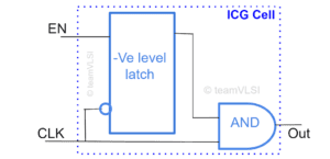
Figure 1 ICG circuit based on latch and AND gate
Preventing glitches is a feature of ICG circuits. ICG circuits based on latches and AND gates perform well in this regard, so this architecture of clock gating circuits is widely used. Although there are various architectures for ICG circuits, this article is limited to discussing this architecture.
Functions of ICG circuit:
Saving power consumption: One of the main functions of the ICG circuit is to reduce chip power consumption by controlling clock signal transmission. In a large-scale integrated circuit, the power consumed by the clock tree can reach a considerable proportion of the overall power consumption. By using ICG circuits, the clock signal can be prevented from propagating to certain logic cells when they are not required to operate, thereby reducing the dynamic power consumption of the clock tree. This capability allows the chip to use energy more efficiently during lighter workloads, extending battery life.
Improved performance: ICG circuitry can improve the performance of the chip under certain circumstances. By clock gating certain logic units, unnecessary clock overhead and clock delays can be reduced, thereby speeding up data transmission and processing. When the logic unit does not need to be operated, turning off the clock signal can avoid wasting clock cycles and improve the chip's working efficiency and response speed.
Reduce noise and power waste: ICG circuits can also reduce clock noise and power waste in the chip. In some cases, clock signals propagate between unwanted logic cells, potentially causing electromagnetic interference and wasted power. By using ICG circuits, clock signal transmission can be effectively controlled to avoid noise interference and unnecessary energy consumption.
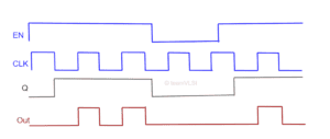
Figure 2 Waveform of ICG unit
As shown above, it provides glitch-free clock-gated output. The clock signal is only passed when the enable signal is high, and clock propagation is stopped when the enable signal is low.
Why can't I use AND gates as clock gating?
First of all, the input of the AND gate will output a high level only when the two conditions of the logical expression are met at the same time. This means that the clock signal will only be passed to the logic unit when all gate signals are high at the same time. In some cases, this can cause problems. For example, in some circuits, a combination of multiple conditions may be required to enable a logic cell. Using an AND gate as clock gating may not satisfy this need because it will only deliver the clock signal when all conditions are met simultaneously.
Second, the use of AND gates may limit design flexibility. In an actual design, it may be necessary to independently control the operation of logic cells under different clock gating conditions. Designs using a single AND gate often require all conditions to be put together, which may complicate the logic and increase maintenance difficulty. In addition, if the gating conditions need to be changed in future solutions, the circuit may need to be redesigned, increasing development costs and workload.
The problem with the AND gate as a clock gating is that it does not provide a glitch-free output, whereas a glitch-free clock wave is highly desirable.
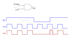
Figure 3 AND gate as clock gating
If the clock enable signal changes when the clock signal is low, it has no impact on the gated clock. However, if the clock enable signal changes when the clock signal is high, glitches will occur in the gated clock. To suppress this glitch, ICG circuits based on latches and AND gates are preferred.
Reference:
[1] https://teamvlsi.com/2021/08/integrated-clock-gating-icg-cell-in-vlsi.html
[2] https://blog.csdn.net/weixin_50518899/article/details/136280198