In today's high-tech field, connection units in physical design play an indispensable role. They are standard units used to connect the inputs of logic gates, providing stable high or low signals. Due to some limitations of transistors, especially on lower technology nodes, high and low level signals cannot be applied directly to the gates of any transistor. Therefore, in this article, I will introduce you to the necessity, schematic, functionality and layout of the connection unit.
Necessity of connecting units:
In lower technology nodes, the gate oxide under the polysilicon gate is very thin and is the most sensitive part of the transistor. We need to pay special attention to this thin gate oxide during manufacturing (a related issue is the antenna effect) and during operation. It has been observed that if the polysilicon gate is directly connected to VDD or VSS to provide constant high/low input signals, and if there are any surges/glitches in the supply voltage, it results in damage to the sensitive gate oxide. To avoid the damage mentioned above, we avoid connecting VDD or VSS directly to the input of any logic gate. The connection unit is used to connect the input of any logic to VDD or VSS.
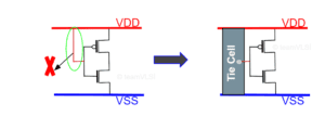
Figure 1 The necessity of connecting units
There are two types of connection units:
- Connect a high unit: the output is always high.
- Connect a low unit: the output is always low.
Schematic diagram of the connection unit:
The design of the connection unit is based on the schematic diagram of the electronic circuit. Common schematic elements and design points of the connection unit will be introduced below.
- Signal lines and pins
In the schematic diagram of the connection unit, the signal line is responsible for transmitting signals, while the pins are the physical interface between the connection unit and other components. Proper design of signal lines and pins ensures free flow of signals between the connection unit and other components. The connection unit has no input pins and only one output pin. The output of a cell connected high is always high and the output of a cell connected low is always low, it is a glitch free output connected to the input of any logic gate. The schematic diagram of connecting high-level cells and connecting low-level cells is shown in Figure 2.
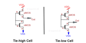
Figure 2 Connect high level and connect low level units
In the connected high unit, the drain and gate of the nMOS are shorted together and connected to the gate of the pMOS, and the output comes from the drain of the pMOS. In the connected low-level unit, the drain and gate of the pMOS are shorted together and connected to the gate of the nMOS, and the output comes from the drain of the nMOS.
buffers and drivers
In order to enhance the reliability and stability of signal transmission, buffers and drivers are often included in the schematic diagram of the connection unit. The buffer can enhance the driving capability and transmission speed of the signal, while the driver is responsible for adapting the levels and currents of different inputs and outputs.Routers and switches
For complex connection unit designs, routers and switches serve as important elements in the schematic diagram to implement the selection and switching of different signal paths. They can flexibly connect different components and provide more complex and flexible signal routing functions.
Connection unit functions:
Connecting a high level unit works similarly to connecting a low level unit. How connecting high level cells works is explained here. Think of connecting low-level units similarly. Connect the high level cell from Figure 2 and the drain and gate of the nMOS are shorted.
So Vg = Vd
==> Vgs = Vds
Therefore, Vds > Vgs -Vt
This indicates that nMOS will always be in the saturation zone. A MOS configuration with the drain and gate shorted is often called a diode connected transistor. While the nMOS behaves as a diode here, the gate of the pMOS is always low, so the pMOS is always on. When a pMOS is on, its drain (output) will always be high.
Similarly, for connecting low level cells, the pMOS is always in the saturation region, so the gate of the nMOS will always be high, so the drain of the nMOS will always be at the low logic level.
It is also important here that sudden fluctuations in VDD or VSS do not propagate to the output of the connected unit.
Layout of connection units:
The layout of the connection units is a key part of the physical design process and directly affects the performance and manufacturing efficiency of the circuit. Here are a few common layout principles and strategies.
Compact layout: refers to arranging connection units as closely as possible to reduce signal transmission distance and delay. Through compact layout, the speed and efficiency of circuits can be improved, space occupied can be reduced, and the density and manufacturing efficiency of integrated circuits can be improved.
Signal grouping and hierarchization: During layout, you can group signals according to their type and transmission characteristics, and place frequently communicating components and signal lines in adjacent locations. At the same time, through hierarchical layout, associated circuit modules can be placed at different levels to improve circuit maintainability and wiring flexibility.
Power and ground wire layout: Proper power and ground wire layout in the connection unit is crucial to the reliability and interference immunity of the circuit. By placing the power and ground wires close to related components and signal lines, the impedance of the power and ground wires can be reduced and circuit interference and noise can be reduced.
Arbitration and scheduling circuit layout: For large-scale connection unit design, a reasonable layout of arbitration and scheduling circuits is required to achieve parallel processing and resource sharing. By placing arbitration and scheduling circuitry close to the components that need to be connected, the flexibility and efficiency of the circuit can be increased.
thank you
[1] https://teamvlsi.com/2021/08/tie-cells-in-physical-design.html