The Decap [Decoupling Capacitor: decoupling capacitor] unit is a special Filler cell. When a large number of units in the circuit flip over at the same time, the instantaneous charge and discharge current will increase, causing the dynamic power supply voltage of the circuit to decrease or the ground voltage to increase, causing a dynamic voltage drop, commonly known as IR-drop. In order to avoid the impact of IR-drop on circuit performance, a capacitor composed of MOS tubes is usually placed between the power supply and the ground line. This capacitor is called a decoupling capacitor or decoupling unit. Its function isWhen the transient current increases or the voltage drops, the current is added to the circuit to maintain the voltage stability between the power supply and the ground wire and prevent the voltage drop of the power line and the increase of the ground wire voltage.。
Schematic and layout of the Decap unit:
MOS transistors can be made into capacitors using various methods, but the most common structure is shown in Figure 1.
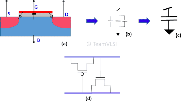
Figure 1 Schematic diagram of MOS capacitor and Decap unit
Figure 1(a) shows the various capacitances inside a MOS transistor. If the source, drain and body terminals are connected together, all these capacitances will be configured as parallel capacitances, as shown in Figure 1(b), and form a single equivalent capacitance, as shown in Figure 1(c). Figure 1(d) shows the Decap capacitor schematic using pMOS and nMOS transistors. From this schematic, we can say that the capacitance caused by nMOS and pMOS will be connected in parallel and add up to form a large capacitor. Figure 2 shows the layout of the simplest Decap unit.
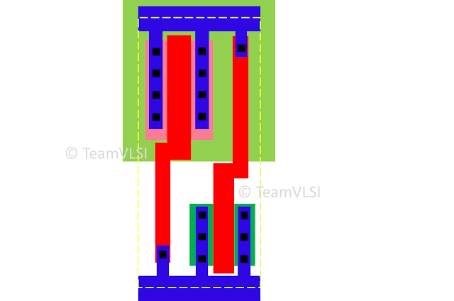
Figure 2 Decap capacitor layout
The source and drain of the pMOS transistor are shorted together and connected to VDD, and the gate is connected to VSS. Likewise, the source and drain of the nMOS transistor are connected to VSS and the gate is connected to VDD.
Use of Decap unit:
There is an input conversion region in CMOS logic operation. In this region, nMOS and pMOS are turned on at the same time, as shown in Figure 3(a). A large short-circuit current Isc will flow instantaneously. If a large number of such cells are placed together and switched together, a large amount of current is required, as shown in Figure 3(b). This high current demand may lower VDD or increase the ground voltage, which is called voltage droop or ground bounce, as shown in Figure 3(c).
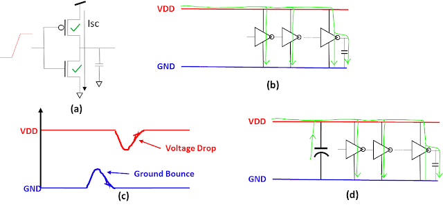
Figure 3 Use of Decap unit
Voltage drops or ground bounces may cause latency changes in connected standard units. Because the delay is proportional to the supply voltage. Variations in latency may further affect the timing of the design, and if the supply voltage drops significantly, the functionality of the standard cell may be affected. Therefore, to support power delivery, we added the Decap unit. The Decap unit acts as a charge reserve pool, supporting the power delivery network and making it more robust, as shown in Figure 3(d).
Decap unit placement:
Decap units are usually placed after power planning and before standard unit placement, that is, during the pre-placement phase. At this stage, place the units evenly throughout the design. Decap units can also be placed in the rear stage if required.
The only problem with Decap units is that they will leak and increase the leakage power of the design, so they must be used with caution.
thank you
Original link:https://teamvlsi.com/2020/08/decap-cell-in-physical-design.html
https://blog.csdn.net/Tao_ZT/article/details/102456733