Flip-flop is the most commonly used sequential component in any ASIC design, especially D-type flip-flops. In a D flip-flop, D stands for delay, meaning the output is a delayed version of the input D. The Latch is the simplest and basic timing component. Generally speaking, two latches are needed to make a flip-flop. Flip-flop is sensitive to clock edges, while Latch is sensitive to clock levels. The following sections explain the internal structure and operation of Flip-flop and Latch. In this article, we will only discuss the most common D-type flip-flop and D-type latch in ASIC design. You can view the link [2] video collection first.
Schematic diagram of Latch and Flip-flop
The simplest designs, Latch and Flip-flop, have 3 pins, an input data pin (D), an input clock/enable pin (CP/E), and an output pin (Q). There may also be setup and reset pins, but for simplicity we do not include these in the discussion. The symbolic representation of Latch and Flip-flop is shown in Figure 1.
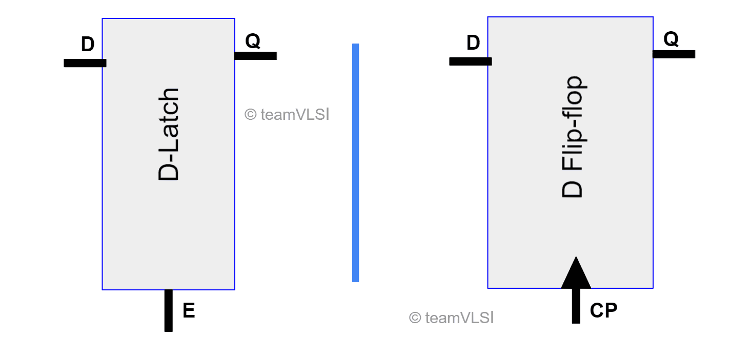
Figure 1 Symbolic representation of Latch and Flip-flop
In Figure 1, the symbols of the positive level-sensitive D-Latch and the symbols of the positive edge-triggered D Flip-flop are shown. In negative latch and flip-flop, only one point appears before the E/CP pin. At a high level, we can think of Latch and Flip-flop as 2:1 multiplexers. Latch can be implemented using a 2:1 multiplexer, while to implement flip-flop, two multiplexers are required. Figure 2 shows the architecture of a positive level-sensitive D-Latch and a positive edge-triggered flip-flop, expressed in the form of a multiplexer.
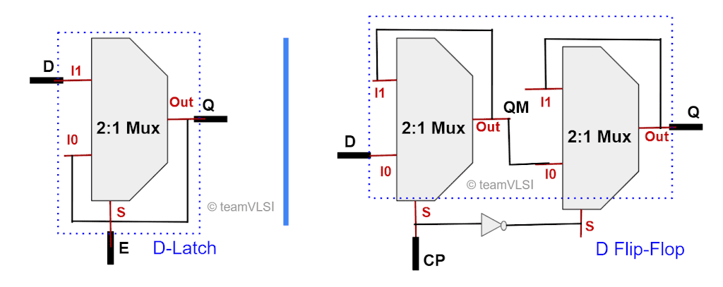
Figure 2 Positive D-Latch and Flip-flop using multiplexer
In a positive-level sensitive latch, the output is fed into the I0 input of the multiplexer, as shown in Figure 2. Likewise, in a negative level sensitive D-Latch, the output Q is fed back to the input I1. A positive edge triggered D flip-flop consists of two negative level sensitive D-Latch connected back to back. In the case of a negative D flip-flop, two positive level sensitive D-Latch are required. If we dig deeper into the multiplexer and go to the transistor level, we find the transistor level schematics of positive level sensitive D-Latch and positive edge triggered D Flip-flops as shown in Figure 3.
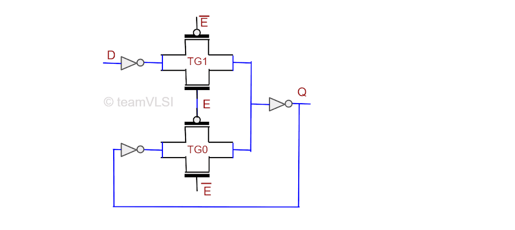
Figure 3.a Positive level sensitive D-Latch using transmission gate
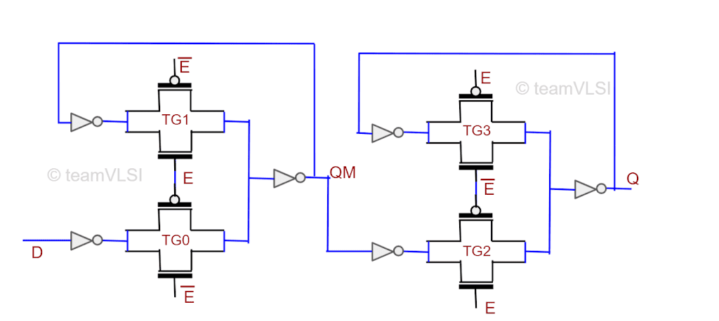
Figure 3.b Use the positive edge of the transmission gate to trigger D Flip-flop
A 2:1 multiplexer consists of two transmission gates made using a pair of pMOS and nMOS transistors as shown in the figure above. A Latch has two transmission gates, one of which has its input connected to its output. Flip-flop consists of two latches (i.e. four transmission gates) connected back to back, as shown in Figure 3. As you can see from the picture above, Flip-flop has more transistors (double) compared to Latch, so Flip-flop has twice the area of Latch. Understanding how Latch and Flip-flop work is the most important part and will be discussed in the next section.
How D-Latch works
Here we only discuss the working principle of positive level sensitive D-Latch, and illustrate it with the help of input and output waveforms. How flip-flop works is discussed in the next section.
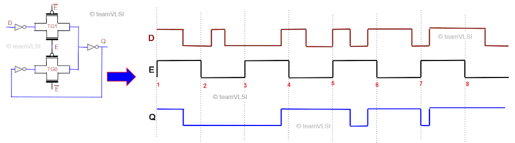
Figure 4 Latch input-output waveform
Two transmission gates are used in D-Latch. In the case of a positive level sensitive D-Latch, the output is fed back to the input of the TGO transmission gate. The transmission gate consists of an nMOS and a pMOS, as shown in the figure above, and is controlled by the enable signal E, which is actually a clock signal. When the enable signal is high, the nMOS and pMOS of TG1 are in the on state, and at the same time, both transistors of TG0 are in the off state, and vice versa. When the enable signal is high, a direct path is established from pin D to pin Q, which is known as the Latch being in a transparent state. But when the enable signal goes low, the TG1 gate is in the off state, establishing a feedback loop from Q to TG0 input to ensure that the output Q does not change when the input pin D changes. This is called the Latch state. Figure 5 shows how Latch works when it is transparent and when it is latched.
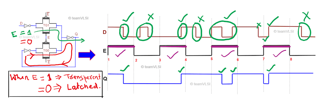
Figure 5 Working principle of positive level sensitive D-Latch
The working principle of the positive level sensitive D-Latch is simple, when its enable signal E is high, it passes the input D to Q, and when the enable signal is low, it keeps the output Q unchanged. As shown in Figure 5, the output only changes when the input changes and the enable signal is high.
How D flip-flop works
In a positive edge triggered D flip-flop, there are two negative level sensitive D-Latch connected back to back, and the enable signal of the second Latch is inverted compared to the first Latch. The inverted enable signal of the second latch ensures that both latches are never in the transparent or latched state at the same time. For better understanding, Figure 6 shows typical input and output waveforms.
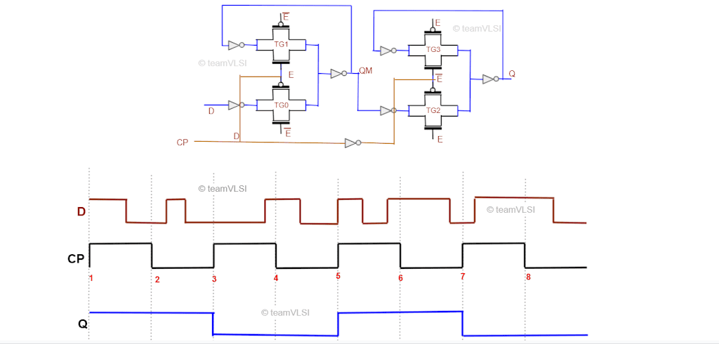
Figure 6 Input and output waveforms of positive D flip-flop
Assume that when the clock signal is low, the first Latch is in a transparent state and input D is transmitted to the QM point. But at the same time, since the inverted clock signal is obtained, the second Latch will be in the latch state, so the output Q will be latched with QM. During this time, the output Q will not change.
At the next instant, when the clock signal transitions from low level to high level, the first Latch will convert from transparent mode to latch mode, and the second Latch will convert from latch mode to transparent mode. Therefore, when the clock transitions from low to high, the signal previously sampled at QM will be transferred to the output Q.
The next instant, when the clock signal is high, the input signal D is no longer transmitted and the signal previously sampled at QM will be available at the output Q.
When the clock signal transitions from high level to low level, the first Latch will convert from latch mode to transparent mode, and the second Latch will convert from transparent mode to latch mode. Therefore, the output does not change at the clock transition edge.
The working of positive D flip-flop can be summarized as the output will only change on the rising clock edge, when the input D will be transferred to the output Q, while at other times the output will remain unchanged. Therefore, it is easier to avoid burrs than Latch, but is larger in area and more susceptible to process variations. Watch this playlist for detailed action and comparison.
Link:
[1] https://teamvlsi.com/2021/08/flip-flop-and-latch-internal-structures-and-functions.html
[2] https://www.bilibili.com/video/BV1oL411D77D/?spm_id_from=333.337.search-card.all.click&vd_source=2ac617c241afd7f9774b0add4e647179