In this article, we will discuss LEF files used in ASIC design. LEF is the abbreviation of Library Exchange Format [Library Exchange Format]. LEF files are written in ASCII format, so this file is readable, and it is provided by foundry.
LEF is a library file necessary for automatic placement and routing. As the process size gradually shrinks, many new physical effects continue to appear in the chip manufacturing process, and the design rules become more and more complex. LEF files are also constantly updated. Currently, the LEF file describing the library mainly has two parts:
- Technology LEF [Technology LEF]: mainly includes process information, design rule information, and industrial control information
- Cell LEF [Cell LEF]: Geometric information containing information about each unit in the cell library
1 Process LEF
The process LEF section contains all metal interconnections, via [via] information, and related design rule information. An example snapshot is provided below showing the information under the Process LEF section.
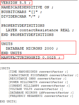
Figure 1 Version, unit
The process LEF section contains the following information:
LEF version(e.g. 5.7 or 5.8)
Unit: Used for conversion between international standard units and LEF database units. Currently, LEF supports four unit conversion factors of 100, 200, 1000, and 2000.
Layer information: Layer name (such as poly, contact, via1, metal1, etc.) + layer type (such as routing, masterslice, cut, etc.) + priority direction (such as horizontal or vertical) + spacing (PITCH) + minimum width (WIDTH) + gap (SPACING) + interconnection layer resistance value (RESISTANCE PRERSQ) + plate capacitance value + edge capacitance value + definition of cumulative antenna effect value.
Interconnect vias: The definition of interconnection vias is composed of cloth layers, including two interconnection layers and a cut layer, classes and rules for selecting vias.
Via array: Connection channels for power, ground, and wider interconnect lines to reduce via resistance. Automatically generated by placement and routing tools based on via rules.
Same-net spacing: DRC checks for routing or verification tools to define minimum gaps within layers.
(1) Three types of layers:
Routing layer: The layer used for wiring, usually contains information such as metal lines and connections, and is used to connect different components on the chip.
Masterslice layer: Represents the main slicing layer, which is used to define the layout information of standard cells and macro cells and plays an important role in chip design.
Cut layer: used to define the cutting area in the metallization layer. It usually contains information about the area that needs to be made into a hole or cut off in the metal layer. It can be understood as an interface connecting two layers of interconnection lines.
A snapshot of the LEF file is provided below, showing the different dimensions of the layer sections and metal interconnects.
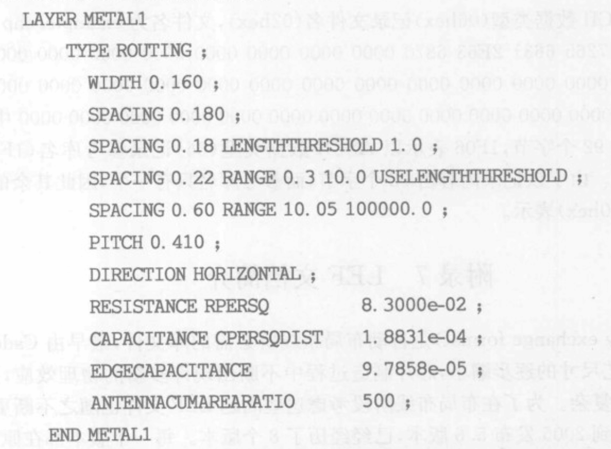
Figure 2 Layer sections and metal interconnects in process LEF
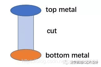
Figure 3 Metal layer and cut layer
(2) PITCH & WIDTH & SPACING
Pitch (PITCH): Indicates the distance between the tracks of each layer. The center line of the component should be stuck on the track for placement. In other words, it is the distance between the center lines of two adjacent components. It is often used to describe the layout of closely packed components or circuit structures. For example, if the pitch between two transistors is 100 nanometers, it means that the distance between the center lines of the two transistors is 100 nanometers.
Minimum width (WIDTH): Indicates the minimum width of a component or circuit structure. It is usually used to constrain the line width or the width of metal lines in chip design. For example, if the minimum width of a certain layer is 20 nanometers, it means that all line widths on this layer cannot be smaller than 20 nanometers.
SPACING: Indicates the spacing or gaps between different components or circuit structures. It is usually used to constrain the minimum spacing between lines and lines and physical objects in chip design. For example, if the gap of a certain layer is specified to be 10 nanometers, it means that the minimum distance between lines on this layer and between lines and other physical objects cannot be less than 10 nanometers.
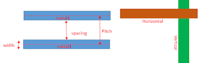
Figure 4 Layer sections and metal interconnect information
(3) Interconnection line via
A complete via is composed of three layers, two interconnect layers and a cut layer. There are a variety of via types available between interconnect lines. The cut layer can be understood as the interface connecting two layers of interconnect lines. Usually, there are multiple through-hole types between each two-layer interconnection lines for the router to choose, and the router selects the most appropriate through-hole to connect the two-layer interconnection lines without violating the DRC.
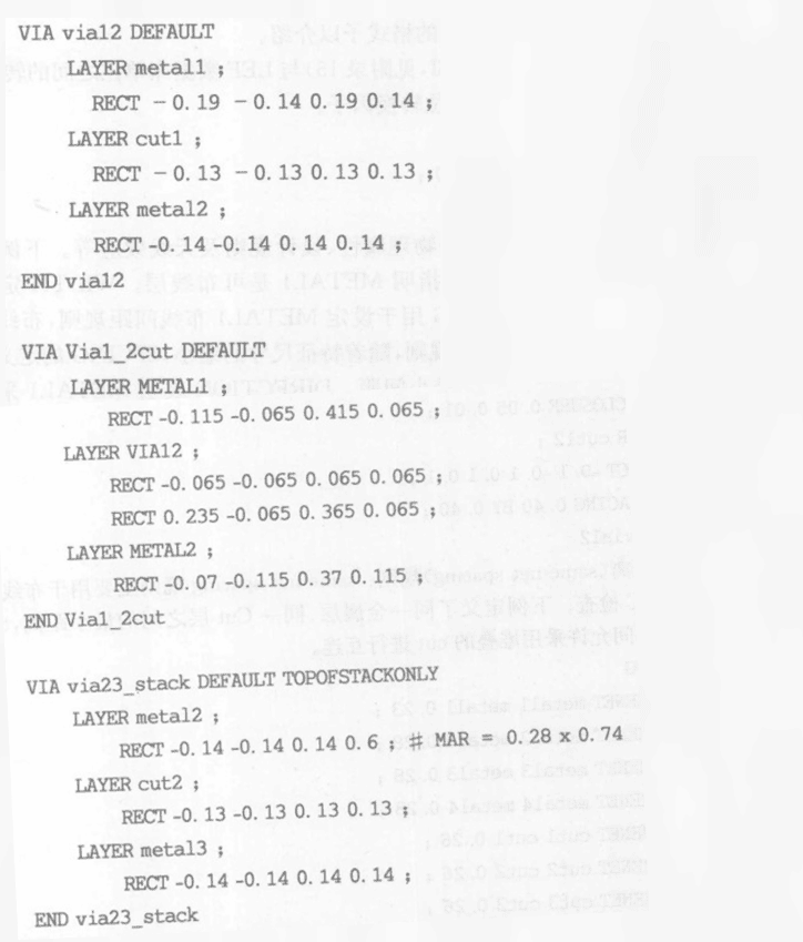
Figure 5 Interconnect vias in process LEF
The above example defines three different types of vias. The first via is named Via12, which is used to connect metal 1 layer and metal 2 layer. It consists of a single cut layer. The second via, named Via_2l2cut, is also used to interconnect metal 1 and metal 2, but this is a via consisting of two cut layers. The third via is named via23 stack, and the TOPOFSTACKONLY statement determines that this via can only be used when vias are stacked.stackThat is, two vias connected up and down can be wired through. The shape of the RECT representation layer is a rectangle. The four values after each RECT represent the X and Y axis coordinates of the lower left corner of the rectangle and the XY axis coordinates of the upper right corner of the rectangle from left to right.
(4)Through hole array
The following example defines a via array named via12. The vias are used to connect the metal layer 2 and the metal layer 3. A cut layer is generated every 0.4 units (X and Y directions). ENCLOSURE defines the distance of the Cut layer from the metal boundary.
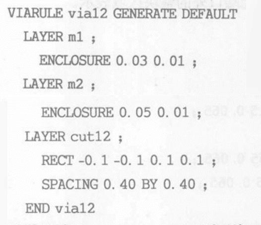
Figure 6 Via array
(5) Same connection distance
The following example defines the minimum distance between the same metal layer and the same cut layer. STACK indicates that stacked cuts are allowed to be interconnected between different metal layers.
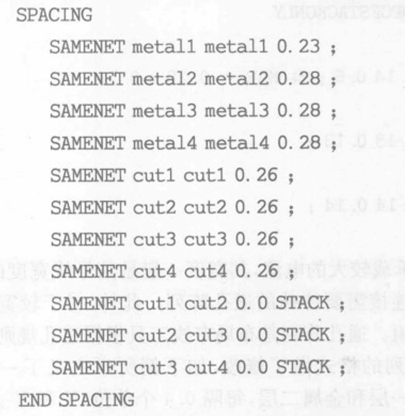
Figure 7 Same connection distance
2 unit LEF
The unit LEF section contains information about each unit in the standard unit library, which is presented separately in different sections. The file can be divided into two parts, one is the definition of the smallest unit of placement using the SITE statement, and the other is the description of the unit attributes and geometric shape using the MACRO statement.
Unit LEF basically contains the following information:
- Unit name (such as AND2X2, CLKBUF1, etc.)
- Category (such as CORE or PAD)
- Origin 0 0
- Dimensions (width x height)
- Symmetry (such as XY, X, Y, etc.)
- Pin information
- Pin name (such as A, B, Y, etc.)
- Direction (such as input, output, bidirectional inout, etc.)
- Purpose (such as signal, clock, power, etc.)
- Shape (usually Abutment for power pins)
- Layer (such as Metal1, Metal2, etc.)
- The rectangular coordinates of the pin (lower left corner llx lly upper right corner urx ury)
(1) SITE statement
SITE defines the smallest layout unit. As shown below, the name of this minimum layout unit tsm12site will be referenced in the SITE definition of the unit (MACRO).
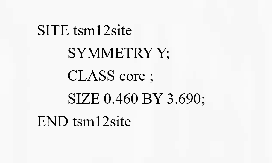
Figure 8 SITE example
The above LEF field defines the size and direction of the site. Size is the horizontal length and BY is the height. The following standard cell will refer to the site definition. The horizontal length of all stardard cells must be an integer multiple of the site length. We do not allow stardard cells that are not integer multiples of the site length.
(2) MACRO statement
MACROis the keyword of unit definition. Each MACRO represents a unit.Class CoreThe description unit is used in the core area of the chip.
FOREIGNDefines the offset between the unit origin coordinates (the coordinates of the lower left corner of the layout) and the reference origin.
ORIGINIt describes the coordinates of the lower left corner of the unit layout. The example shows that the coordinates of the lower left corner are the coordinates of the origin.
SIZEThe area size of the unit is determined. The example shows that its length in the X direction is 5.980 and its height in the Y direction is 3.690.It can be seen that 5.98 is an integer multiple of site0.46.
SYMMETRYXYIt means that the unit can be placed symmetrically along the X-axis and Y-axis.
SITE statement within MACROThe specified unit uses the predefined tsm12site as the minimum layout unit.
everyPIN statementRepresents a port of the unit. The description includes the input and output properties of the port, its purpose, and the metal layer and metal shape used by the port.
OBSIt is the non-routable area of the unit. For standard units, the non-routable area usually refers to the area represented by all other interconnection layers of the unit except the unit port. For satellite modules, the non-routable area is usually represented by the entire area except the unit port. For example, a snapshot of a MACRO statement is provided below to better understand the format.
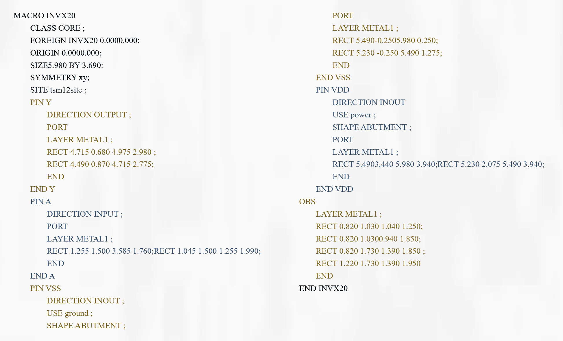
Figure 9 MACRO example
LEF files are used by routing tools in place-and-route [PnR] designs to obtain the locations of standard cell pins so they can be routed correctly. So it's basically an abstraction of the standard cell layout.
5 quotes
[1] "Physical Design of Digital Integrated Circuits" P243-248
[2] https://teamvlsi.com/2020/05/lef-lef-file-in-asic-design.html