In this article, we will discuss a widely used and very popular file used to transfer data from one Electronic Design Automation (EDA) tool to another. Yes, we will be discussing Design Exchange Format or DEF files, which have a .def extension. In this article, we will discuss the use of def files, what information this file contains and how the information is arranged in the various sections.
DEF is first generated for layout planning. As an input file, it is successively input into layout and routing and then perfected. It will eventually be converted into a GDS layout for physical verification. After passing it, it will be tape-out.
1 Introduction
DEF files are used to represent the physical layout of an integrated circuit (IC) in ASCII format. DEF files are closely related to Library Exchange Format [LEF] files. Therefore, both files are necessary for the physical design to display correctly. The DEF file format was developed by Cadence Design System. Whenever we need to transfer the design database from one EDA tool to another for further implementation or analysis, we use DEF files to transfer the design data. For example, when performing IR analysis or STA analysis on a PnR database, we transfer the design database in the form of a DEF file.
The DEF file contains specific design information of the circuit. It is a representation of the design at any node in the physical design process. It not only includes the connection relationship of the circuit, but also describes the specific physical information of the units and interconnection lines after the circuit layout and wiring. DEF conveys logical design data and physical design data.
Logical design data includes internal connectivity (represented by the netlist), group information, and physical constraints. Physical data includes component placement and orientation and routing geometry.
2 parts
A standard DEF file mainly contains the following parts, and the order of declarations is also important.
[VERSION statement]
[DIVIDERCHAR STATEMENT]
[BUSBITCHARS STATEMENT]
[DESIGN statement]
[ TECHNOLOGY STATEMENT ]
[UNITS Statement]
[DIAAREA Statement]
[ROW statement]
[TRACKS Statement]
[CELLGRID STATEMENT]
[VIAS Statement]
[ NONDEFAULTRULES statement ]
[ COMPONENTS STATEMENT ]
[PINS SECTION]
[BLOCKAGE PART]
[FILLS section]
[ SPECIALNETS SECTION ]
[NETS section]
[SCANCHAINS part] #scanchain
[GROUPS section]
[BEGINEXT part]
[END DESIGN statement]
Here we will take a sample DEF file and describe the various parts of the file.
(1) Title [HEADER] statement:
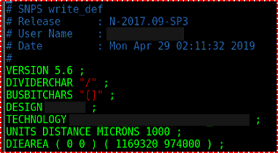
Figure 1 Title declaration of DEF file
In the title section, the DEF version, design name, technology name, units and wafer [Die] area are mentioned.
Unit (UNIT) is used to convert between SI units and DEF database units.
Design name (DESIGN), corresponding to END DESIGN, the description of the design in DEF is included between DESIGN and END DESIGN.
Chip area (DIEAREA) determines the chip area size.
(2) Row [ROW] statement:
The layout area composed of multiple small SITEs is called a row. The width of a standard unit is usually an integer multiple of a SITE, so the layoutable area of a unit is composed of many rows composed of SITEs. SITE is defined in a LEF file, refer back to the 2.3 LEF file. Each row in the chip is described in DEF.
Syntax:
[ROW rowName siteName origX origY siteOrient [DO numX BY numY [STEP stepX stepY]] [+ PROPERTY {propName propVal} …] … ;] …
Here is an example of the line [ROW] section of a DEF file.
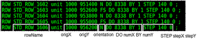
Figure 2 Line description of DEF file
rowName: Specifies the row name of the row.
siteName: Specifies the LEF node used for this row.
origX and origY: Specify the position of the first node in the row.
siteOrientation: Specifies the orientation of all nodes in the row.
Do numX BY numY:
- Specifies the set of duplicate nodes that create this row.
- One of the values must be 1.
- If numY is 1, the rows will be horizontal.
STEP stepX stepY:
- Specifies the spacing between nodes in horizontal and vertical rows.
(3) Track [TRACK] statement:
Routing tracks used to describe the design.
Syntax:
[TRACKS [{X | Y} start DO numtracksSTEP space [LAYER layerName…] ;] …]
Example:
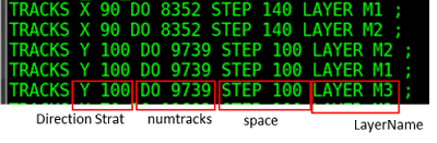
Figure 3 Track statement in DEF file
Description:
{ X | Y } start
- Specify the direction and position of the first track
- X represents vertical line, Y represents horizontal line
- The starting point is the X or Y coordinate of the first line
- The starting track starts at the start number
Do numtracks
- Specify the number of tracks to create in the grid
STEP space
- Specify the spacing between tracks
LAYER layerName
- Specifies the routing layer to use for this track
- We can specify multiple layers
(4) Global cell network [GCell Grid] statement:
Syntax:
[GCELLGRID {X start DO numColumns+1 STEP space} … {Y start DO numRows+1 STEP space ;} …]
Example:

Figure 4 GCell statement in DEF file
Description:
{ X | Y } start
- Specifies the position of the first vertical (x) and first horizontal (y) rails
Do numColumns+1
Do numRows+1
- Specify the number of columns or rows in the grid
STEP space
- Specify the spacing between tracks
(5) Through hole [VIA] statement:
Example:
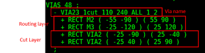
Figure 5 Via statement in DEF file
Description:
All vias are composed of shapes on three layers
cutting layer
Two routing (or master) layers connected by this cut layer
(6) Non-default rule [NDR] statement:
Syntax:
NONDEFAULTRULES numRules; {- ruleName [+ HARDSPACING] {+ LAYER layerName WIDTH minWidth [DIAGWIDTH diagWidth] [SPACING minSpacing] [WIREEXT wireExt] } … [+ VIA viaName] … [+ VIARULE viaRuleName] … [+ MINCUTS cutLayerNamenumCuts] … [+ PROPERTY {propNamepropVal} …] … ;} … END NONDEFAULTRULES
Example:
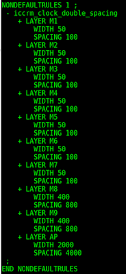
Figure 6 NDR in DEF file
Description:
It defines any non-default rules used in this design that are not specified in the LEF file.
This section can also contain default rules and LEF non-default rule definitions for reference.
(7) Component [COMPONENTS] section:
Describe the physical properties of the unit after layout.
- Define design components, their locations and related properties
- A large section of a DEF file
Syntax:
COMPONENTS numComps; [– compNamemodelName [+ EEQMASTER macroName] [+ SOURCE {NETLIST | DIST | USER | TIMING}] [+ {FIXED pt orient | COVER ptorient | PLACED ptorient | UNPLACED} ] [+ HALO [SOFT] left bottom right top] [+ ROUTEHALO haloDistminLayermaxLayer] [+ WEIGHT weight] [+ REGION regionName] [+ PROPERTY {propNamepropVal} …]… ;] … END COMPONENTS
Example:

Figure 7 Components section in DEF file
The first row shows that COMPONENTS has a total of 274722 units.
icc_clock is the name of the unit in the design, followed by the model name of the unit in the library. PLACED is the coordinate position where the unit is placed on the chip, and the last letter indicates the orientation of the unit.
(8) Pin [PINS] part:
- Define external pins
- Each pin definition is assigned a pin name for the external pin and associates the pin name with the corresponding internal network name
- The pin name and net name can be the same.
example:

Figure 8 Pin section in DEF file
(9) Obstacle [BLOCKAGE] part:
- Define placement and routing of obstacles in your design
- PUSHDOWN: Specifies that obstacles are pushed downward from the top level of the design
Example:
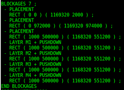
Figure 9 Obstacle part in DEF file
(10) Special line [SPECIAL NET] part:
Syntax:
[SPECIALNETS numNets; [– netName [ ( {compNamepinName| PIN pinName} [+ SYNTHESIZED] ) ] … [+ VOLTAGE volts] [specialWiring] … [+ SOURCE {DIST | NETLIST | TIMING | USER}] [+ FIXEDBUMP] [+ ORIGINAL netName] [+ USE {ANALOG | CLOCK | GROUND | POWER | RESET | SCAN | SIGNAL | TIEOFF}] [+ PATTERN {BALANCED | STEINER | TRUNK | WIREDLOGIC}] [+ ESTCAP wireCapacitance] [+ WEIGHT weight] [+ PROPERTY {propNamepropVal} …] … ;] … END SPECIALNETS]
Example:
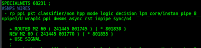
Figure 10 Special network section in DEF file
(11) Network [NETS] part:
NETS describes the connection netlist of signal interconnection lines. In addition to the basic connection relationships, it can also include the physical attributes of each signal line, such as the frequency, capacitance size, and function of the interconnection line. The definitions of signal interconnects are contained in the keyword NETS.
Syntax:
NETS numNets; [– { netName [ ( {compNamepinName| PIN pinName} [+ SYNTHESIZED] ) ] … | MUSTJOIN ( compNamepinName) } [+ SHIELDNET shieldNetName] … [+ VPIN vpinName[LAYER layerName] ptpt [PLACED pt orient | FIXED ptorient | COVER ptorient] ] … [+ SUBNET subnetName [ ( {compNamepinName| PIN pinName| VPIN vpinName} ) ] … [NONDEFAULTRULE rulename] [regularWiring] …] … [+ XTALK class] [+ NONDEFAULTRULE ruleName] [regularWiring] … [+ SOURCE {DIST | NETLIST | TEST | TIMING | USER}] [+ FIXEDBUMP] [+ FREQUENCY frequency] [+ ORIGINAL netName] [+ USE {ANALOG | CLOCK | GROUND | POWER | RESET | SCAN | SIGNAL | TIEOFF}] [+ PATTERN {BALANCED | STEINER | TRUNK | WIREDLOGIC}] [+ ESTCAP wireCapacitance] [+ WEIGHT weight] [+ PROPERTY {propNamepropVal} …] … ;] … END NETS
Example:
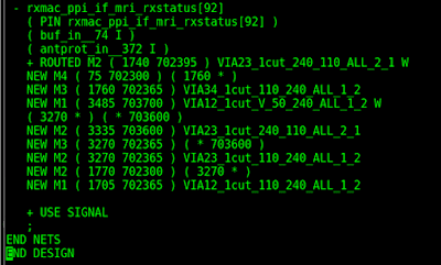
Figure 11 Network section in DEF file
"rxmac_ppi_if_mri_rxstatus[92]": This is the name of the signal network, indicating the role or function this signal network plays in chip design.
"(PIN rxmac_ppi_if_mri_rxstatus[92])(buf_in_74 I)(antprot_in_372 I)": This part describes where the signal comes from and where it goes. "(PIN rxmac_ppi_if_mri_rxstatus[92])" means that the signal is output by the pin named "rxmac_ppi_if_mri_rxstatus[92]", "(buf_in_74 I) (antprot_in_372 I)" means that the signal is input to the buffer (buffer) numbered 74 and the antenna protector (antenna protector) numbered 372.
Next is the specific wiring information:
"+ ROUTED M2( 1740 702395 ) VIA23_1cut_240_110_ALL_2_1 W": Indicates that the signal passes through layer M2, from coordinates (1740, 702395) Connected to a via named VIA23_1, a cut operation with a width of 240 and a height of 110 was used, with cut mode ALL, direction 2 (horizontal), index 1, towards W.
"NEW M4(75 702300)(1760*) NEW M3(1760 702365 ) VIA34_1cut_110_240_ALL_1_2": Indicates that the signal passes through layer M4, from coordinates (75, 702300) to (1760, 702365), connected via a via named VIA34, using a cut operation of width 110, height 240, cut mode ALL, direction 1 (vertical), and index 2.
The subsequent section "NEW M1( 3485 703700 ) VIA12_1cut_V_50_240_ALL_1_2 W(3270*)(*703600)" describes the final part of the signal path, connecting layer M1 and the corresponding via, using cutting operations and metal filling.
3 Distinguish the concepts of pitch, spacing, width, site, row and track
Pitch & spacing & width & track are the concepts of wiring. The tracks routed on each metal layer are divided into vertical and horizontal ones. The width of the track is width, the distance between the center lines of the two tracks is pitch, and the gap between the two tracks is spacing.
site & row is the concept of layout. The site is defined in the LEF file and defines its width and height. The height of standard units is fixed, that is, the height of the site, and the width of the standard unit is required to be an integer multiple of the site. Several sites form parallel lines, and these parallel lines are rows.
Quote
[1] https://teamvlsi.com/2020/08/def-file-in-vlsi-design-exchange.html
[2] LEF/DEF Language Reference